Currency
Toggle Nav

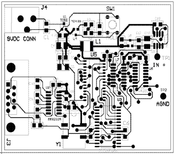
Engineering issues that need attention in the manufacturing of PCB
September 20, 2017
1. Avoid the input end getting too close to the output end, especially in the case of high gain.
For the following reasons:
1) When it is a positive amplifier, being too close would generate the parasitic capacitance - positive feedback loop – then cause the shock; this shock is independent of the input signal, that is, it could happen without input. The frequency of this shock depends on the circuit structure and parasitic capacitance and other factors, most of the time it’s over 1MHz. However, with the changes of parasitic capacitance, what would be caused is not only the circuit shock, sometimes the situation of work instability and deterioration would happen.
2) When it’s the opposite amplifier, the Miller effect is generated, which would cause the deterioration of high-frequency characteristics, then form the LPF (signal resistor Rg and Miller capacitance (A + 1) C). Miller effect: The output signal has an A times increase to the input signal and is inverted. When the input and output exist in capacitor C , seen from the signal source, it could be seen as if the phenomenon that there exists (A+1)C capacitor between the input and GND. Summary: whether the positive phase amplification or reverse amplification, the input end and output end are not allowed to be close to each other, especially in high-gain or in the wideband amplifier! At the same time, when using multi-stage amplifier, the same security measurements should be taken.
 2. The lines with large difference in electrical level don’t get too close (the difference at above 30 ~ 40dB), even if the DC is not allowed because of the similar reason, high-voltage voltage ripple may be coupled to the weak signal side, thus make the performance of the weak signal side deteriorated, but also may occur such as shock and other anomalies.
3. Distinguish the small signal GND and high current GND.
Reasons: due to the presence of resistance in GND, a large current flowing will produce a voltage drop. This voltage drop has little effect on the high current side, but improves the potential of the small signal GND, which also makes the characteristics get worse.
Summary: Connect all the points of the high current GND together, and connect all the points of the small signal GND together, and then connect these two points together. Besides, the line carrying a large current should be small resistance and thick as much as possible.
4. Power GND line needs to be distributed to each substrate.
Reasons: when the circuit is complex, it would be divided into several substrate modules, but the power supply is only one, so if the power supply is connected to a substrate module, and then the power of the other substrate is supplied from the power supply of the last substrate, and so on. At this time, because of the existence of resistance in each section of the power cord, so, as long as one of the modules’ current changes (the current of the sink GND increases, the GND voltage drop flowing the sink current would grow, that is, the ground potential of those modules is increased - the supply voltage is reduced), this will make the power supply voltage of all modules changed!
2. The lines with large difference in electrical level don’t get too close (the difference at above 30 ~ 40dB), even if the DC is not allowed because of the similar reason, high-voltage voltage ripple may be coupled to the weak signal side, thus make the performance of the weak signal side deteriorated, but also may occur such as shock and other anomalies.
3. Distinguish the small signal GND and high current GND.
Reasons: due to the presence of resistance in GND, a large current flowing will produce a voltage drop. This voltage drop has little effect on the high current side, but improves the potential of the small signal GND, which also makes the characteristics get worse.
Summary: Connect all the points of the high current GND together, and connect all the points of the small signal GND together, and then connect these two points together. Besides, the line carrying a large current should be small resistance and thick as much as possible.
4. Power GND line needs to be distributed to each substrate.
Reasons: when the circuit is complex, it would be divided into several substrate modules, but the power supply is only one, so if the power supply is connected to a substrate module, and then the power of the other substrate is supplied from the power supply of the last substrate, and so on. At this time, because of the existence of resistance in each section of the power cord, so, as long as one of the modules’ current changes (the current of the sink GND increases, the GND voltage drop flowing the sink current would grow, that is, the ground potential of those modules is increased - the supply voltage is reduced), this will make the power supply voltage of all modules changed!
 Summary: It could be solved by connecting the power supplies of all the substrate modules in parallel to the power supply module.Of course, we can also visit pcb assembly this page, look for your solution online.
5. The flowing direction of current should be taken into account for electrolytic capacitor.
The reason is: for the filter capacitor, such as the regulator capacitor after the transformer, in the actual wiring, if the lead wire is from the bridge rather than from the regulator capacitor, then the load current will directly flow to the load circuit without flowing through the filter capacitor, this will result in the voltage with obvious voltage ripple, and the greater the load current is, the larger the filter capacitor.
Summary: pay much attention to the actual current flowing direction when wiring. The current must first flow into the capacitor, and then out of the capacitor, this is the right flowing direction and will maximize the effect. At the same time, this is also effective for the power supply bypass capacitor.
6. Reduce the area of current loop.
Reasons: the bigger the current loop area is, the greater it could be impacted by the external magnetic field and other factors. The conduction wires of other loops will produce the magnetic field, the greater the area of the loop is, the more magnetic wires it could pass through - the greater impact on the original circuit it will make.
Summary: whether it is signal line or power cord, try to make its area as small as possible, it’s the best to use twisted pair if possible! Otherwise, try to make its area small.
7. Largely separate the power supply circuit, power circuit and small signal circuit from each other.
Reasons: the small signal circuit is susceptible to other circuits, and the electrical level of the signals processed by the power supply circuit and power circuit is large, which is easy to affect other circuits. In the power supply circuit, the transformer is the main source of noise as well as the leakage of magnetic, so pay attention to the direction of transformer installation.
8. Place the dual transistor / FET as close as possible.
Reason: the semiconductor is extremely sensitive to the temperature. If the circuit is designed in the premise of the transistor and FET characteristics being the same, then it is expected to make the temperature of chip close to the thermal coupling as much as possible.
9. Keep heat-affected devices away from heat sources and there is a need of considering the flowing of hot air.
10. Note the operability of the actual circuit board installation, commissioning and other operations. For instance: 1. If the location of hole opening(screws) touched the nearby conductive wires. 2. For the components (rheostats, variable capacitors, etc.) that need to be adjusted, if there remained enough space for the use of tools. 3. is sufficient to use the debugging tool. 3. Check if there is enough space for installing the radiator.
manufacturing of pcb
Summary: It could be solved by connecting the power supplies of all the substrate modules in parallel to the power supply module.Of course, we can also visit pcb assembly this page, look for your solution online.
5. The flowing direction of current should be taken into account for electrolytic capacitor.
The reason is: for the filter capacitor, such as the regulator capacitor after the transformer, in the actual wiring, if the lead wire is from the bridge rather than from the regulator capacitor, then the load current will directly flow to the load circuit without flowing through the filter capacitor, this will result in the voltage with obvious voltage ripple, and the greater the load current is, the larger the filter capacitor.
Summary: pay much attention to the actual current flowing direction when wiring. The current must first flow into the capacitor, and then out of the capacitor, this is the right flowing direction and will maximize the effect. At the same time, this is also effective for the power supply bypass capacitor.
6. Reduce the area of current loop.
Reasons: the bigger the current loop area is, the greater it could be impacted by the external magnetic field and other factors. The conduction wires of other loops will produce the magnetic field, the greater the area of the loop is, the more magnetic wires it could pass through - the greater impact on the original circuit it will make.
Summary: whether it is signal line or power cord, try to make its area as small as possible, it’s the best to use twisted pair if possible! Otherwise, try to make its area small.
7. Largely separate the power supply circuit, power circuit and small signal circuit from each other.
Reasons: the small signal circuit is susceptible to other circuits, and the electrical level of the signals processed by the power supply circuit and power circuit is large, which is easy to affect other circuits. In the power supply circuit, the transformer is the main source of noise as well as the leakage of magnetic, so pay attention to the direction of transformer installation.
8. Place the dual transistor / FET as close as possible.
Reason: the semiconductor is extremely sensitive to the temperature. If the circuit is designed in the premise of the transistor and FET characteristics being the same, then it is expected to make the temperature of chip close to the thermal coupling as much as possible.
9. Keep heat-affected devices away from heat sources and there is a need of considering the flowing of hot air.
10. Note the operability of the actual circuit board installation, commissioning and other operations. For instance: 1. If the location of hole opening(screws) touched the nearby conductive wires. 2. For the components (rheostats, variable capacitors, etc.) that need to be adjusted, if there remained enough space for the use of tools. 3. is sufficient to use the debugging tool. 3. Check if there is enough space for installing the radiator.
manufacturing of pcb