Currency
Toggle Nav

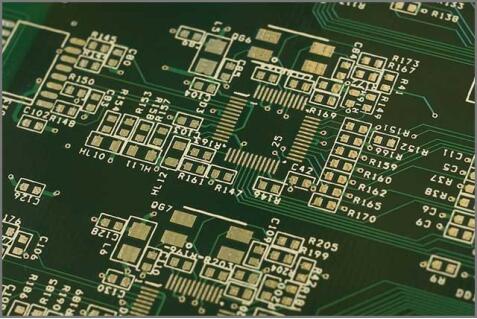
10 Points You Need to Know in PCB Design for Manufacturing
August 03, 2022

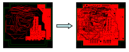
In the next few days, we will publish an article series about PCB design and manufacturing process. Detailed guidance will be elaborated on what should be paid attention to during PCB designing and manufacturing. Let’s get started with the first topic- PCB design. Designing is the first step in PCB manufacturing. PCB design covers many aspects and involves many details. Generally speaking, it involves 10 aspects: PCB thickness design, laminated structure design, inner graphic design, borehole design, outer circuit design, solder mask design, PCB form factor design, PCB multi-pieces splicing design, V-CUT design and PCB thermal design.
PCB thickness design
- The allowable plate thickness of general mounting machineis during 5~5mm. PCB thickness is generally within the range of 0.5~2mm. Only when assembling low-power components such as integrated circuits, low-power transistors, resistors, capacitors and under the condition of no strong load vibration, the thickness of PCB is 1.6mm, and the size of the board is within 500mm × 500mm;
- Under the condition of loaded vibration, the method of reducing the size of the plate or strengthening and increasing the support points should be adopted according to the vibration conditions, and the 1.6mm plate can still be used;
- When the plate surface is large or cannot be supported, it can be considered to increase the plate thicknessto 2~3mm. When the PCB size is smaller than the minimum mounting size, the splicing method must be adopted.
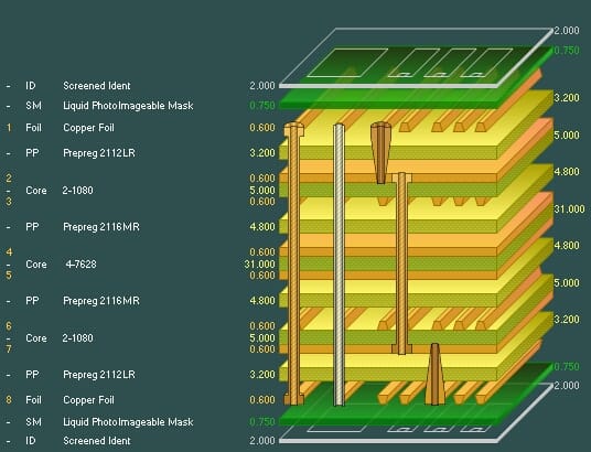
Design of laminated structure
The basic design principles of laminated structure are:
- If the customer has a designated structure, it willbe designed according to the customer's requirements.
- When the customer has impedance requirements, the laminated structure that meets the customer willbe used.
- When the customer does not specify the structure, the design principle is: the thickness of the dielectric layer and the pressing thickness meet the customer's requirements.
- The core board with larger thickness is preferred for the inner board.
Inner graphic design
The graphic copper of each layer shall be evenly distributed to prevent warping. The graphic structure between layers shall be evenly distributed as far as possible, and symmetry shall also be considered for layer sequencing. The distance from the inner hole to the line should be increased as much as possible. The higher the level, the greater the distance. (4 layers of plates shall be more than 7mil, and 6-8 layers shall be more than 8mil)
The higher the level, the greater the distance from the inner hole to the copper, generally more than 10mil, so as to improve the reliability. In the area with dense holes, the line shall be arranged in the middle of the two holes as far as possible.
Design of boreholes
Mechanical mounting hole:
If it is not used for grounding, electroplated coating is not allowed on the inner wall of the mounting hole.
If grounding is required, it is recommended to design "guard holes" around the installation hole.
Component hole:
The diameter of the metalized hole is 0.2~0.3mm larger than the diameter of the lead, which is conducive to the solder of wave soldering to climb up and is conducive to exhaust the gas at the same time. If the hole is too small, the gas cannot escape and will be mixed in the solder. The hole is too large, and the element is prone to deflect.
Through hole:
The principle of hole selection is try to use through holes, followed by buried holes, and finally select blind holes. Try not to cross when designing blind buried holes.
Design of outer circuit
- The minimum safety distance between the elements of the outer layer of NC milling and the plate edge is 0.25mm. No through holes shall be arranged on the SMD pad, and the distance between the through holes and the pad shall be 0.2mm.
- When the wiring of the whole design is completed, try to lay copper on the blank area without wiring to increase the anti-interference power of the circuit. Draw the outline of the copper pouring area, select the pouring method, and connect the ground network with the copper sheet. However, the distance between copper sheet and pad and wire should better be at least8mil.
- The uniform distribution of outer copper can make the current distribution and coating thickness uniform during electroplating, which is convenient for production and processing and conducive to product reliability.
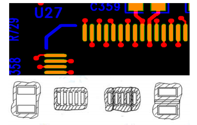
Solder mask design
- The Through hole treatment method is to cover the plug hole, but it is best not to put the via that needs to be plugged on the pad of the window, in order to avoid oil generation, resulting in abnormal welding, such holes are covered without plugging the hole treatment.
- To prevent short circuits caused by solder bridging, it is often necessary to retain the green oil bridge. When the IC pad spacing < 8mil, the green oil bridge cannot be retained.
- The maximumdiameter of the plug hole is 0.6mm, it is recommended that the via bore diameter of the plug hole needed to be designed within 0.6mm, and the best one is between 3-0.4MM. For example, in order to ensure good conduction, a few more holes can be placed with the network.
- The viaholes in the BGA area are processed in the form of plug holes without special requirements. When designing test points, it is recommended to identify them with identification numbers on the character layer.
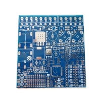
PCB form factor design
The shape of the printed board should be as simple as possible, like rectangular. The length-width ratio is 3:2 or 4:3, and its size should be the standard size so as to simplify the processing process and reduce the processing cost. The plate surface should not be designed too large so as not to cause deformation during reflow soldering.
The form and size of the PCB are determined by the PCB transmission mode and the mounting range of the mounting machine. When the PCB is positioned on the placement table and the PCB is transmitted through the workbench, there are no special requirements for the shape of the PCB. When the PCB is transmitted directly from the guide rail, the PCB shape must be straight. If it is a special-shaped PCB, the process edge must be designed to be a straight line.
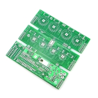
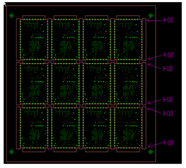
PCB multi-pieces splicing design
When the PCB size is less than the minimum mounting size (<50mm×50mm), it must be designedin the form of a panel, and the special-shaped board also needs to be plated.
The splicing designcan improve production efficiency. When adopted double-sided full surface mounting without using the wave soldering, It can be designed with a double-numbered panel, half of the front and back sides, and the same graphics on both sides. This design can use the same template to save the programming and production preparation time, improving production efficiency and equipment utilization.
Splicing design requirements:
- The size of the panel should not be too large, nor too small. It should be determined according to PCB (The maximum panel size of the PCB with a thickness of 1mm is 200mm × 150mm)
- The edge of thesplicing boards is generally 5-10mm, and the positioning hole should be
- The markpoint is added to the diagonal part of each small board.
- The positioning hole is added to the process side, and the distance is 5mm from each side. Asymmetrical 3-4 positioning holes can be added to the process edge.
V-CUT Design
There is no spacing between the process edges and the unit board. When the width of the bridge is small, then we resort to V-CUT design. There are several angles of V-CUT : 20°, 30°, 45°, 60°. The most commonly used is 30°.
V-CUT residual thickness:
- Plate thickness<1.6MM residual thickness 0.3+/-0.1MM.
- Plate thickness≥1.6MM residual thickness 0.4+/-0.1MM.
PCB thermal design
High-heat devices and the radiator should be considered to be placed in the air outlet or somewhere conducive to convection. The PCB is laid out with high-heat components in mind at the air outlet or in a location conducive for convection. Temperature-sensitive devices should be away from heat sources. If the required distance cannot be reached due to spacing reasons, the temperature rise of the temperature-sensitive device should be guaranteed to be within the derating range through temperature testing.
Related Products