Currency
Toggle Nav

ALL About Multilayer PCBs You Should Know
1. What is Multilayer PCB?
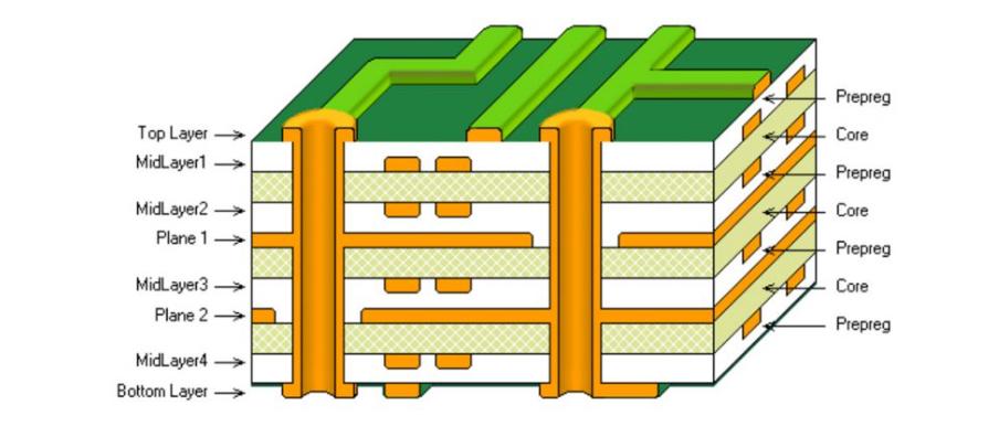
Compared to the traditional single-layer PCB, multilayer PCBs consist of 3 or over 3 layers of conductive copper foils. A Double-Sided PCB has two conductive layers on top and bottom of the PCB substrate. The top and bottom layers of a multilayer PCB look like that of a double-sided PCB but there are more layers on both sides of the core. They often appear as Many layers of double-sided circuit board glued and laminated together with layers of heat-protective insulations. Copper-plated holes interconnect these layers, and electric connections from the middle of the layers are obtained from vias such as blind and buried vias, plating through holes.
On the top and bottom layers of the multilayer PCB, there are active and passive components placed while the inner stacked layers are used for routing. It is arranged so that on the PCB, two layers are placed on the surface to connect the environment. Both through-hole electronic components and Surface Mount Components (SMD) can be soldered on either side of this type of PCB. SMD components can be soldered with Surface Mount Technology and other PCBA Tools. By applying such methods, producers can construct different sizes of highly complex PCBs.There can be up to 40 layers for multilayer PCBs.
2. Single-Layer vs.Double-sided PCBs vs.Multilayer PCBs: What's the Difference?
Single-layer boards, also known as single-sided PCB have just one layer of base material, also known as a PCB substrate.
Double-sided PCBs or double-layer printed circuit boards, as the name suggests, are more complicated than Single Sided PCBs as they consist of one single layer of the base substrate with 2 conductive (copper) layers on both sides of the substrate. There are solder masks applied on both sides of the board as well.
The definition of a multilayer PCB is a PCB that is made with three or more conductive copper foil layers. Once you look closer at the three primary types of PCB boards, you'll see there are many other differences in how they're constructed and how they function.
1). Single-Layer PCB
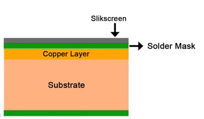
Single-layer boards, sometimes called single-sided boards, have components on one side of the board and a conductor pattern on the opposite side. They have just one layer of conductive material, typically copper. A single-layer board is comprised of a substrate layer, a conductive metal layer, and then a protective solder mask and silk screen. You'll find single-layer boards in many simpler electronic devices.
2). Double-Sided PCBs
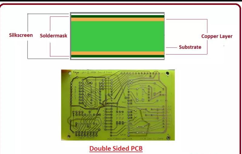
You can also use a double-layer or double-sided board, which has more layers than a single-layer board but fewer than a multi-layer. Double-sided PCBs, like the single-sided variation, have one substrate layer. The difference is that they have a layer of conductive metal on both sides of the substrate.
Circuits and components on one side of the board are connected to those on the other side through one of two methods:
- Through-Holes: Through-holes are small holes drilled through the board that wires, called leads, are fed through, then soldered to the correct component.
- Surface Mounts: These PCBs use leads soldered directly to the board. The board itself becomes the wiring surface for the components, which allows the circuits to take up less space.
3). Multi-Layer PCBs
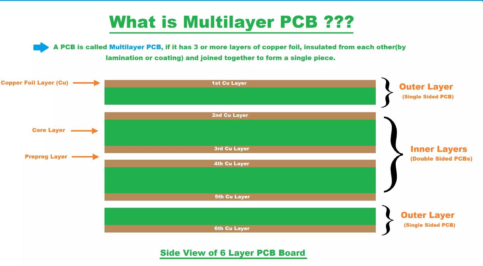
Multi-layer PCBs are made of three or more double-sided boards stacked on top of each other. Theoretically, they can contain as many boards as you can need, but the largest one ever made was 129 layers thick. Typically, they have an even number of between four and 12 layers — odd amounts can cause problems such as warping and twisting post-soldering.
Each substrate layer in a multi-layer board has a conductive metal on both sides of it. The boards are joined together using a specialized kind of adhesive, and there is an insulating material between each board. On the very outer edges of the multi-layer board, you'll find solder masks.
Multi-layer boards typically appear in more complex devices that require a high number of connections.
Paths known as vias allow the different layers to conduct to each other. These paths fall into three groups: Through-Hole, Blind via, and Buried via, see more details about them below.
3. What is a Multiplayer PCB Via?
To put it simply, via refers to an electrical connection between different layers on the printed circuit board. Vias come in three types: through-hole vias, blind vias, and buried vias.
Through-hole Via- Go through every layer of the board
Through-hole vias also known as standard vias pass through all layers of the printed circuit board to connect the top, bottom, and inner layers. Their dimensions are larger than those of other via types, and drilling is not restricted.
Blind Via-Connect an outer layer to an inner layer
The blind vias are typically drilled from the outside layer of the printed circuit board to the inner layers without making a hole on the other side of the board. For the holes cannot be seen from another side of the board, they are referred to as ‘’blind” vias.
Buried Via-Connect two inner layers, rendering them invisible from the outside
Buried vias connect two or more inner layers of the printed circuit board and are not visible on either outer layer. In the production of multilayer PCBs, the internal plating of the buried vias must be completed before applying the two outer layers of the board. As they require to be designed more precisely, the Manufacturing cost will increase for buried vias.
4. Multilayer PCB Manufacturing Process
For there are more chances of cross connections, overlaps, tracing in copper areas, etc. It’s detailed and patience-needing work to produce multilayer PCBs and the whole manufacturing process requires special precaution. The whole process needs to be finished in an SD(electrostatic discharge)-Safe and Cleanroom environment. Special manufacturing setup and equipment are needed for the 8+ layer PCB manufacturing process.
Here are the basic steps involved in Multilayer PCB Manufacturing Process:
Design -The process starts with designing the Layout of the PCB using any PCB designing software / CAD Tool (Proteus, Eagle, OrCAD).
Making the Inner Layer Core - Laminate of desired thickness is treated with Copper foil, dry film resistance, and UV light to make the inner layer core.
The lamination - This process includes the Inner layer core, prepeg sheets, and copper foil sheets. The sheets of material are staked on each other and holes are used to align them as they are stacked up.
For a 4-layer board, the Staking of layers is as follows: Bottom Layer of Copper Foil – Prepeg Sheets – The Inner Layer Core – More Prepeg Sheets – Finally Copper Foil Sheet on Top.
Applying pressure - heat and vacuum using a heated hydraulic press. The vacuum is important to make sure there is no air trapped between the layers. This process ends over 2 hours depending on the number of layers.
Forming - Once cured, resins from the prepegs join the sheets, core, and foil together forming a multilayer PCB.
See the tech and processings applied in multilayer PCB production here:
Cutting -The process of cutting the original copper-clad board into a board that can be made on the production line.
Inner Dry Film-The inner dry film is the process of transferring the inner circuit pattern to the PCB board.
Black Oxidation-The boards with inner layer wiring must be blackened or browned before they can be laminated. It is to oxidize the copper surface of the inner layer board. It is used to add mild corrosion resistance, for appearance, and to minimize light reflection.
Lamination-Lamination is the process of bonding layers of circuits into a whole using B-stage prepreg.
Mechanical Drilling-Mechanical drilling is to use a drill to cut at high speed to form a through hole in the PCB.
Metalize The Through Hole-The metallization of the hole is to solve the problem of covering the cross-section with a uniform, thermal shock-resistant metal copper.
Dry Film & Pattern Plating - The outer layer graphics transfer is similar in principle to the inner layer graphics transfer. Both use photosensitive dry film and photographic methods to print circuit patterns on the board.
Solder Mask -The solder mask process is to add a layer of solder mask on the surface of the board for protection against oxidation and to prevent solder bridges from forming between closely spaced solder pads.
The specific process is as follows: Pre-treatment-> coating one> pre-bake-> exposure-> development-> UV curing-> thermal curing.
Silkscreen - Silkscreen is a layer of ink traces used to identify components, test points, parts of the PCB, warning symbols, logos, marks, etc.
Surface Finished-The most basic purpose of surface treatment is to ensure good solderability or electrical properties.
Profiling -The process of PCB profile is to cut PCBs from a working panel to be set or individual Pcs according to the customer's requirement, normally there are three types of PCB profile in the PCB manufacturing process, the most popular one is milling, also known as routing, the second one is V-Cut, and the third one is punch.
E-TEST -The electronic test is the electrical performance test of the PCB, which is usually also called the "on" and "off" test of the PCB.
Final inspection - Inspection methods usually include Optical inspection, target inspection confirmation, and visual inspection confirmation to confirm or eliminate some true and false defects.
Package - The main packaging types are Anti-Static Packaging, Moisture-Proof Packaging, and Anti-Vibration Packaging, but the usual packaging only uses vacuum packaging.
5. Advantages of a Multilayer PCB
- Small Size: For their layered design, multilayer PCBs are more compact than other PCBs with the same functions. Multilayer PCBs wield great advantages in modern electronics, as smaller, more compact yet more powerful gadgets like smartphones, laptops, tablets, and wearables now usher in the new trend.
- Less Noisy:The RF(Radio Frequency) designs, including antennae of high-speed signals and high-frequency signals, need a good grounding shield. On the other hand, multilayer PCB permits the user to place separate ground and power planes so that RF components can receive a better ground shield, hence, the noise gets reduced.
- Lightweight Construction:A smaller PCB weighs less, with multiple layers laminated together with electronic components arranged orderly, room and weight saved, making up more space for a complicated electronic application.
- High-Quality: Due to the tech iteration, research, and development put into the creation of multilayer PCBs, these types of PCBs tend to perform better in quality than single and double-sided PCBs.
- More Durable:Multilayer PCBs tend to be durable by their nature. Not only do these multilayer PCBs have to withstand their own weight, but they must also handle the heat and pressure used to bind them together.
- More Flexible:mThough this does not apply to all multilayer PCB assemblies, some do use flexible construction techniques, resulting in a flexible multilayer PCB.
- More Powerful:Multilayer PCBs are extremely high-density assemblies, combining multiple layers into a single PCB. These close quarters enable boards to be more connective, and their innate electrical properties allow them to achieve greater capacity and speed despite their smaller size.
- Single Connection Point: Multilayer PCBs are designed to work as a singular unit, rather than in tandem with other PCB components. As a result, they have a single connection point, rather than the multiple connection points required to use multiple single-layer PCBs.
These merits make multilayer PCBs excel, with so many industries stepping into mobile solutions, multilayer PCBs are taking a really significant role in many industry-specific applications.
6. Disadvantages of a Multilayer PCB
- Higher Cost: Multilayer PCBs are significantly more expensive than single and double-layer PCBs at every stage of the manufacturing process.
- Complicated Production: Multilayer PCBs are more difficult to produce, requiring much more design time and careful manufacturing techniques than other PCB types.
- Limited Availability:One of the largest issues with multilayer PCBs is the expenses of the machinery needed to produce them. Not all PCB manufacturers have the funds or the necessity for this machinery, so not all PCB manufacturers carry it.
- Skilled Designer Required:As previously discussed, multilayer PCBs require extensive design beforehand.
- Increased production Time:each board requires a significant amount of time to produce, resulting in more labor costs. Additionally, it possibly leads to longer periods between when an order is placed and when the product is received, which can be a problem in some circumstances.
However, these issues do not diminish the utility of multilayer PCBs. While they tend to cost more than a single-layer PCB, a multilayer PCB claims many advantages over this type of printed circuit board.
7. Applications of Multilayer PCB
Multilayer Printed Circuit Boards offer more flexibility and enhanced circuit density with reduced size. This is why these boards can be used in many electronic applications:
Computers and Laptops - Due to their high-performance and space-saving features, Multilayer PCBs can be applied for manufacturing electronic components from server to motherboard mainly. With low cost, Multilayer PCB wields a big role in those applications above. Besides, Multiplayer PCB can be a large support for file servers and data storage-related tech devices.
Telecommunications Equipment – With good functionality and durability, multilayer PCBs are often used in telecommunication devices such as satellites, GPS, mobile phone repeaters, and signal transmission applications. In the telecommunication industry, PCBs are often used in outdoor towers and mobile devices. In modern applications, durability is vital in maintaining functionality at a high level.
Medical Equipment: Testing, X-Ray, Heart Monitors, CAT(Computerized Axial Tomography) Scan- By dint of their lightweight, small size, and intensive functionality as compared with single-layer options. Multilayer PCBs are broadly used in the medical industry. Multilayer PCBs boost the performance of electronic applications like CAT scans, X-Rays, heart monitor equipment, and medical testing devices.
Military and Defense Equipment-Owing to their exceptional functionality, durability, saving space, and low-weight properties, multilayer PCBs have made their way to military applications even like atomic and nuclear Systems requiring high-speed circuits.
Automotive-The automobile industry has ushered in a new era in the tech industry these days, from electric cars, car computers, GPS, and engine sensors to headlight switches, all the production for the above need high-performance, space-optimizing, compact-size, heat-resistant PCB boards, thus multiplay PCBs have become favored while many automobile manufacturers have opted for multilayer PCBs over other options.
Aerospace- And so forth, the aerospace industry also relies heavily on multi-layer PCBs. From computers used in the control room to those used in the cockpit, PCB applications are reliable as it requires handling the atmospheric journey’s stress while making space for other surrounding equipment. In this way, multilayer PCBs with many protective layers made from flexible materials have been the ideal choice to safeguard the connections from getting damaged by heat and outside stress.
Industrial Equipment -Multilayer PCBs have become the optimal choice over other market options for their durability. They can be utilized in the rough working environment in day-to-day life. From control systems to computers, multilayer PCBs are used in manufacturing industries to run pieces of machinery.ss
A lot more to go! Multilayer PCB is also used in many other industries, including securities, home appliances, and even the science and research industry. From weather analysis equipment to atomic accelerators, fiber optic sensors, and alarm systems, multilayer PCBs are used due to space and weight-saving properties and their high functionality.
8. Elecrow: A Trustful Multilayer PCB manufacturer
As much as it is essential to choose the suitable PCB material, the significance of selecting the proper PCB manufacturer couldn't be denied. Elecrow PCB has proven to be one of the best China PCB assembly manufacturers offering the finest multilayer PCBs.
The best part is that you will have your choice of PCB manufactured, keeping the application of your PCB in line. We always consider the requirements of our clients, and after a thorough discussion and assessment of the PCB application, we develop multilayer PCBs for them.
We focus on quality, appropriate bonding within the PCB structure, and cost-effectiveness. Hence this allows us to provide our clients with a perfect PCB choice that lasts longer and help them reduce the assembly cost as well as minimize space requirements.
Request Multilayer PCB Instant Quote