Currency
Toggle Nav

Guide to Learning About Blind and Buried Vias PCB
PCBs are everywhere. These are called printed circuit boards and are used in almost all industries that manufacture products working with electricity. However, there is depth in the context when you study these PCBs.
PCBs are equipped with various components, and these are all connected. There are plenty of layers of the PCBs too, that allow it to function efficiently. The term blind and buried vias is also a very commonly heard term for PCBs, and if you want to know about these terms, you must read through them below.
In this article, we have discussed everything you might look forward to learning about blind and buried vias and their significance in PCB manufacturing.
Introduction to Blind and Buried Vias in PCB
What is Vias?
Before we dig into the details about the blind and buried vias, you must first understand what vias are. Well, there are multiple layers in PCB. Some have two, and some might have more depending upon the requirement and purpose.
These vias are connected with the help of holes that are copper plated. These holes tend to secure one layer to another layer in the PCB. The holes are first drilled on the board, and electrolysis is carried out to electroplate the holes.
However, the vias occupy space on the board, which may cause space problems. To deal with this problem, the designers tend to use blind and buried vias in their PCBs.
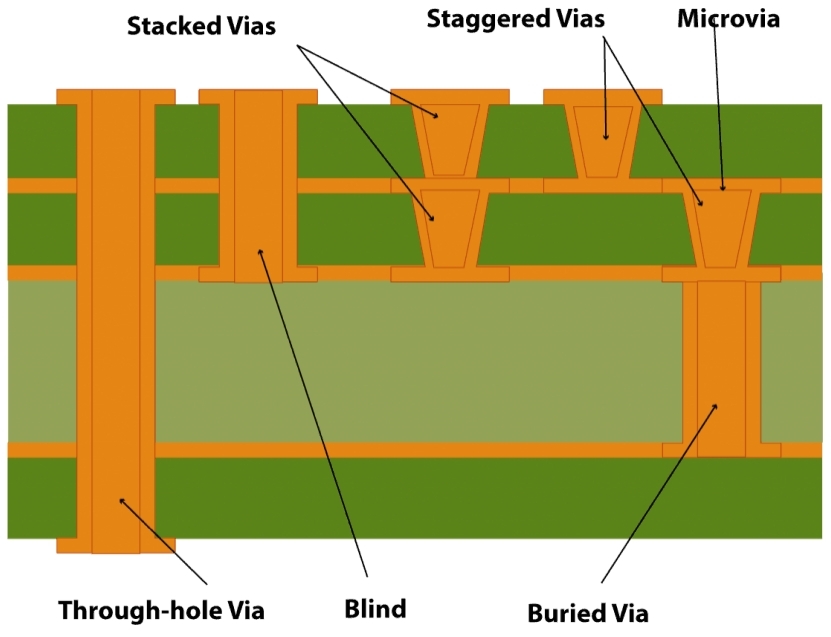
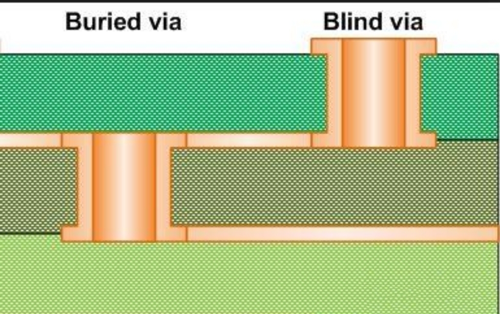
What is meant by blind via PCB?
The blind via creates a link between the internal layers of the PCB. These vias never continue to pass throughout the entire board. The base layer has a connecting layer on the top or the bottom of the board, which is connected using blind vias.
There are many types of blind vias, and each of them has a different purpose for serving. Some of the common types of blind vias may comprise the following:
- Photo Defined Blind Vias PCB
The photo-defined blind vias are created by adding a coat of resin to the PCB core. This core comprises the lamination on the planes, making the layers. This resin applied layer is left to harden, and the unwanted resin on the holes is removed. Once the material is scraped away, the plating process of copper is carried out.
- Blind Via with Sequential Lamination
The blind via sequential lamination is manufactured so that a piece of thin lamination is passed through the holes by drilling these holes in the layers of the PCB. The product then passes through the same process, creating more and more layers.
- Blind Vias through Laser Drilling
In these kinds of vias, the layers of the board are maintained, and then the vias are inserted on the surface. The excessive copper can be removed through carbon dioxide, creating multiple layers.
What is buried via PCB?
Buried vias are also used to connect the layers of a PCB, but these vias do not pass through the outer layers and create a connection within the internal layers only. The bruised vias are developed by drilling the holes and then plating them with the copper on the inner side, which tends to create a multi-layer PCB.
What are Stacked and Micro Via?
Stacked vias can either be blind or buried, and they are also laminated. These vias can connect multiple layers on the PCB and therefore are named stacked vias. These vias are topped over one another and hence look like they are being stacked up.
Similarly, when it comes to micro vias, as the name suggests, these vias are very tiny and might need a microscope to take a look at them. These vias are very commonly used in HDI PCBs because of their smaller size and can be fixed easily on the board without space issues.

However, there lies one problem with these vias: they need more time for drilling, and the hole being drilled leaves the center and may be displaced.
How Blind and Buried Vias are Made in PCB?
The manufacturing of vias can be done in two ways: one is before putting all the layers, and the other is after putting all the layers. The holes are first drilled, and then the electroplating process starts.
The depth of the drill is significant when creating the vias, no matter whether they are buried or blind vias. If the hole is too deep, the signal might go through distortion. In case the hole is shallow, the connection might not remain stable and not work correctly. Hence care must be exercised when it comes to creating vias.
Pros and Cons of Buried and Blind Vias
Everything comes with specific pros and cons, and similarly, when it comes to PCB as well, there are some advantages and disadvantages associated with the blind and buried vias as well.
The benefits of the blind and buried vias include the fact that you can add more components without the need to increase the board's size or the count of the layer.
However, on the other hand, adding these vias also increases the cost of the PCBs, which is a problem for some products because the cost of the product also increases.
Blind Via PCB Applications
By way of using blind vias, you get a chance to expand the getaway channel of the ball grid, and this helps you in minimizing the layers of the PCB at the same time. On the other hand, it also allows you to reduce your ratio of the circuit board aspect. When you have an increased gateway channel, this ratio tends to decrease.
Elecrow: The reliable China PCB manufacturer
As much as it is essential to choose the right PCB consisting of blind and buried vias, the significance of selecting the proper China PCB manufacturer cannot be subsided. Elecrow offers to provide you with the ultimate solution to order your choice of PCB according to your specifications.
No matter which industry you are in and what your electronic products are, by choosing Elecrow, you can have the PCB that suits your needs.
We even aim to provide customized PCBs according to your specifications and allow you to manufacture them efficiently. So, get in touch with us today and have your PCBs designed with us to incorporate into your products.
Request Blind and Buried Vias PCB Instant Quote