Currency
Toggle Nav

3 Common Automation Solutions for PCB Assembly
July 21, 2025
Top 3 Automation Technologies in PCB Assembly
The rapid development of the semiconductor industry over the past few decades is not just a testament to Moore's Law but also a demonstration of the extreme complexity and precision of the entire electronics supply chain. From smartphones and cloud computing to the Internet of Things (IoT), Artificial Intelligence (AI), and 5G communication, these disruptive applications are built on increasingly sophisticated and powerful chips and circuit boards. This trend presents unprecedented challenges to the Printed Circuit Board Assembly (PCBA) industry: how can more components be integrated into smaller areas? How can the flawless quality of thousands of solder joints be guaranteed?
In the face of these challenges, automation is no longer an option but a necessity. It is the lifeblood determining a company's survival and growth. Automation is more than just a tool for reducing labor costs; it is the cornerstone for achieving high-quality, high-efficiency, and high-reliability production. It significantly shortens production cycles, enhances process precision and consistency, minimizes human error, and liberates workers from tedious, repetitive, and even hazardous work environments.
This article delves into the three core automation solutions that play a pivotal role in the modern PCBA industry, analyzing how they collectively build efficient and intelligent electronic manufacturing facilities.
Automatic Test Equipment (ATE)
Automatic Test Equipment (ATE) serves as the quality gatekeeper on the PCBA production line. It has evolved from simply testing individual semiconductor devices into a complex system designed to automatically perform comprehensive electrical validation and defect detection on entire circuit boards during and after the assembly process. Its primary objective is to identify and isolate all potential quality issues before a product moves to the next stage or reaches the customer.
Specific Applications of ATE in the PCBA Industry:
In the PCBA domain, ATE encompasses several specialized types of equipment for different testing stages:
- In-Circuit Test (ICT): After SMT (Surface Mount Technology) and wave soldering, ICT uses a bed of nails to contact test points on the board. It verifies that the values of individual components (like resistors and capacitors) are correct and checks for soldering defects such as shorts and opens. For high-volume production, ICT is exceptionally efficient.
- Flying Probe Test: For prototypes, small batches, or boards with high-density test points, a flying probe tester eliminates the need for expensive custom fixtures. Its mobile probes can flexibly access any solder joint to perform tests similar to ICT, offering outstanding flexibility.
- Functional Test (FCT): This is the test that most closely simulates the product's real-world operation. FCT powers up the board and runs specific software or inputs signals to verify that the board's overall functionality meets design specifications—for example, confirming a communication module can transmit and receive signals correctly.
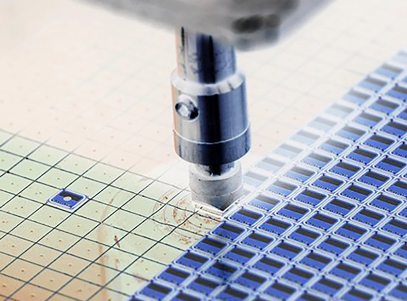
- Automated Optical Inspection (AOI) & Automated X-ray Inspection (AXI): These vision-based systems are also part of the broader ATE category. AOI is used to inspect component placement accuracy and solder joint appearance. For components with bottom-terminated connections like BGAs, AXI can penetrate the chip to inspect the quality of the internal solder balls.
pcb technology
Core Advantages of ATE in the PCBA Industry:
The true value of ATE lies in "early detection, early resolution." By precisely locating a specific faulty component or solder joint in the initial stages of production, it dramatically reduces the cost and complexity of subsequent repairs. Compared to manual inspection, ATE provides unparalleled speed, accuracy, and repeatability, ensuring every PCBA leaving the factory meets stringent quality standards. This is critically important for high-reliability sectors such as automotive electronics and medical devices.
Manufacturing Execution System (MES)
If ATE is the quality gatekeeper, then the Manufacturing Execution System (MES) is the "brain" and "central nervous system" of the smart PCBA factory. It is a powerful software platform that connects, monitors, manages, and optimizes the entire production process in real-time, from raw material receiving to finished goods shipment.
Specific Applications of MES in the PCBA Industry:
On a highly complex PCBA production line, the value of an MES is unmistakable:
- Comprehensive Traceability: An MES can record every component used on each PCBA (even tracing back to its supplier batch), the solder paste, the operator, the production equipment, and the process parameters. If a quality issue arises, it enables immediate reverse traceability to pinpoint the exact scope of affected products for precise recalls and analysis—a lifeline in modern manufacturing.
- Intelligent Material Management: The MES prevents operators from loading incorrect materials onto the line. During SMT setup, when an operator scans a component reel's barcode, the system automatically verifies it against the current work order, preventing material mix-ups at the source. It also monitors the floor life of Moisture-Sensitive Devices (MSD) and the expiration of solder paste.
- Real-time Process Monitoring and Feedback: MES integrates test data from AOI, SPI (Solder Paste Inspection), and ATE. When a defect rate shows an abnormal trend, the system can automatically trigger alerts or even lock down the production line, forcing engineers to investigate. This shifts the paradigm from "post-production inspection" to "in-process prevention."
- Paperless Production and Dispatching: MES digitizes work orders, Standard Operating Procedures (SOPs), and other documents, pushing them in real-time to terminals at each workstation. This ensures workers always use the latest revisions and automatically logs the completion of each process step.
Core Advantages of MES in the PCBA Industry:
By providing a "single pane of glass" view of the production floor, an MES eliminates information silos. It empowers managers with real-time visibility into line efficiency (OEE), Work-in-Progress (WIP) levels, and quality status, enabling more informed decision-making. For high-density, high-mix PCBA production, the granular management capability of an MES is essential for ensuring smooth, efficient, and zero-defect manufacturing.
Robotics
Robotics represents the "hands" that translate MES commands and process requirements into precise physical actions. In the PCBA industry, the application of robotics extends far beyond articulated robot arms to include a variety of highly automated, specialized equipment.
robotics
Specific Applications of Robotics in the PCBA Industry:
- Pick-and-Place Machines: These are the heart of the SMT line and are a form of highly specialized robots. At incredible speeds and with micron-level precision, they pick minute components like resistors, capacitors, and complex chips from feeders and accurately place them onto designated pads on the PCB. This is fundamental to achieving high-density assembly.
- Robotic Placement for Odd-Form Components: For components like connectors and transformers that cannot be handled by standard pick-and-place machines, specialized placement robots can mimic human actions to perform precise gripping and insertion.
- Automated Guided Vehicles (AGVs) & Autonomous Mobile Robots (AMRs): In large factories, AMRs are responsible for automatically transporting PCB racks and component reels from the warehouse to the production line or transferring them between different process steps, enabling fully automated logistics.
- Selective Coating and Dispensing Robots: To protect circuit boards from moisture and chemical corrosion, a conformal coating is applied. Robots equipped with spray nozzles can follow complex paths to perform precise and uniform selective coating, avoiding contamination of areas like connectors that must remain uncoated.
Core Advantages of Robotics in the PCBA Industry:
The core advantages of robotics lie in their ultimate precision, consistency, and tireless performance. When handling micro-components like the 01005 package (measuring just 0.4mm x 0.2mm), the stability and accuracy of a human operator cannot compare to a machine. Furthermore, robots can operate 24/7 in environments requiring strict Electrostatic Discharge (ESD) protection or high cleanliness levels. They also relieve workers from processes involving potential chemical exposure, such as coating and soldering, thereby significantly enhancing both production safety and efficiency.
In the modern semiconductor and PCBA industries, Automatic Test Equipment (ATE), Manufacturing Execution Systems (MES), and Robotics are not isolated solutions but form a synergistic and tightly integrated ecosystem. The MES acts as the brain, issuing production commands and monitoring the overall process. Robotics serve as the hands and feet, precisely executing material handling, placement, and assembly tasks. ATE functions as the eyes and senses, rigorously verifying the quality output of each process and feeding data back to the MES. It is the seamless integration of these three pillars that makes the high-volume, high-quality production of dense and complex PCBAs possible. Without automation, the manufacturing industry would struggle to meet today's insatiable demand for miniaturization and functional integration in electronic products, and quality control would become an insurmountable challenge. Therefore, automation is not merely a key to the success of the semiconductor and PCBA industries; it is the powerful engine driving their continuous innovation and, by extension, the entire technological world forward.