
In the world of modern PCB assembly, two core component mounting technologies dominate: Surface Mount Technology (SMT) and Through-Hole Technology (THT). SMT utilizes automated pick-and-place machines to rapidly affix tiny, leadless Surface Mount Devices (SMDs) onto the surface of a circuit board, which are then secured via reflow soldering. This method is the mainstream for large-scale, high-density PCB assembly. THT, on the other hand, requires components with long metal leads—of which the Dual In-line Package (DIP) is the most iconic example—to be "inserted" through pre-drilled holes in the board and then soldered into place.
This, however, gives rise to a natural question: in an era where SMT is remarkably efficient and highly automated, why has the relatively cumbersome and often manual DIP assembly process not only survived but remained a fixture in nearly all complex electronic products?
The answer is that the continued application of the DIP assembly process is not a sign of technological lag, but rather a deliberate choice driven by engineering realities and product requirements. The strategic value it offers directly compensates for the limitations of SMT in specific scenarios. The persistence of manual DIP assembly is based on several irreplaceable advantages:
- Superior Mechanical Strength: For components subjected to high mechanical stress, such as connectors and switches, THT provides a physical bond far more robust than surface mounting can achieve.
- Compatibility with Special Components: Certain components that are incompatible with automated processes due to their size, weight, irregular lead shapes, or thermal sensitivity must be handled manually.
- Cost-Effectiveness for Low-Volume Production: In prototyping and small-batch manufacturing, the flexibility and low initial investment of manual processes offer unparalleled economic benefits.
Therefore, a deep understanding and mastery of the manual DIP assembly process are essential for guaranteeing the overall quality and long-term reliability of a vast range of electronic products.
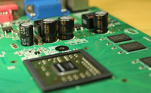
DIP component into PCB
Integrated Execution of the Standard Process Flow
Within the broader PCB assembly workflow, a high-quality DIP process is a coherent and rigorous sequence of operations, interconnected from component preparation to final inspection.
The entire flow begins with the Component Preparation stage. Operators must precisely verify all parts against the Bill of Materials (BOM) and perform lead forming on certain components, ensuring the bend point is at least 1.5 to 2.0 mm from the component body to prevent mechanical stress. The subsequent Insertion phase follows a logical "low-profile to high-profile" sequence and requires strict adherence to PCB silkscreen markings to ensure the correct orientation of polarized components. The entire pre-processing and insertion workflow must be conducted in an Electrostatic Discharge (ESD) safe environment.
Once components are correctly seated, the process seamlessly transitions to the most technically demanding stage: Soldering. The success of this step is directly dependent on the precise control of core process parameters. After soldering is complete, Post-Soldering Processing is required, which includes trimming the leads on the back of the PCB to a standard height of 1.0 to 2.0 mm and thoroughly cleaning any residual flux to prevent potential corrosion or short circuits.
The Core Craft of Soldering: Critical Data and Parameter Control
The quality of the soldering is the cornerstone of the entire DIP assembly process. To achieve stable and reliable solder joints, strict adherence to the critical process parameters listed in the table below is mandatory. This table clearly outlines the standard range for each data point and the engineering purpose behind it.
| Process Parameter | Technical Requirements & Data | Purpose & Explanation |
|---|---|---|
| Soldering Iron Temperature | Leaded Solder: 330°C - 370°C Lead-free Solder: 350°C - 400°C |
A temperature that is too low will cause a cold solder joint, while one that is too high risks damaging the component or PCB pad. Lead-free solder requires a higher temperature due to its higher melting point. |
| Soldering Time | 2 - 4 seconds per joint | This ensures the solder can fully wet the joint without transferring excessive heat that could cause irreversible damage to the component. It is a critical test of the operator's skill. |
| Solder Amount | Solder should cover over 75% of the pad area, forming a smooth, conical shape. | Insufficient solder weakens the connection, while excessive solder can cause shorts. An ideal joint allows the contour of the component lead to be visible. |
| Use of Flux | A suitable amount of flux must be applied to the joint area before soldering. | Flux removes oxides from the metal surfaces and enhances the wetting action of the molten solder, a prerequisite for creating a bright, sound solder joint. |
Quality Inspection: Ideal Solder Joint Criteria and Common Defect Identification
The final quality inspection serves as the last line of defense in ensuring a product meets its reliability standards. An ideal solder joint should be bright and smooth with a well-defined, concave conical shape, exhibiting good wetting on both the component lead and the solder pad, and free of any structural flaws.
During inspection, operators and quality inspectors must be proficient in identifying common soldering defects. The following is a detailed analysis of four typical defects:
- Cold Solder Joint
This is an extremely insidious and hazardous defect. Visually, a cold solder joint lacks its characteristic metallic luster, instead presenting a dull, grayish, and grainy or pasty appearance. Its contour is not well-formed, and it fails to create a smooth wetting angle with the pad and lead, appearing merely "piled on." The root cause is insufficient heat during the soldering process—either the iron temperature was too low or the application time too short—preventing the solder from fully melting and forming a proper intermetallic bond. A cold joint has very low mechanical strength and an unreliable electrical connection that can fail intermittently due to temperature changes, vibration, or minor physical stress, making it a "time bomb" for product reliability.
- Solder Bridge
A solder bridge is a blatant and severe defect where excess solder unintentionally connects two or more adjacent leads or pads that should be electrically isolated, forming a "bridge." This is typically caused by applying an excessive amount of solder or by improperly moving the soldering iron, dragging molten solder across a gap. The consequences of a solder bridge are catastrophic, as it alters the circuit's original design. This can lead to logic errors, signal crosstalk, or even a direct short from power to ground, which can instantaneously destroy sensitive components and, in serious cases, pose a safety risk.
- Solder Peak (or Spire)
A solder peak refers to a joint that fails to form a smooth, conical top, instead featuring a sharp, icicle-like protrusion. This defect is primarily caused by poor operator technique, most commonly by withdrawing the soldering iron too quickly or at an improper angle before the solder has fully solidified, thereby "pulling" up a portion of the semi-molten solder. While a joint with a solder peak may still be electrically conductive, it is considered a process defect. The sharp point significantly reduces clearance distances to other conductors, increasing the risk of arcing in high-voltage environments or shorting due to dust and moisture accumulation over time. It also indicates a lack of process stability.
- Overheating Damage (Thermal Damage)
This is a severe defect that causes permanent physical damage to the circuit board or the component. Its manifestations are varied: mild cases may show discoloration (yellowing or charring) of the solder mask around the pad; severe cases can result in the pad blistering, lifting, or delaminating entirely from the substrate due to adhesive failure. The component itself may show signs of its plastic casing melting, deforming, or cracking. The sole cause is uncontrolled heat—either the soldering iron temperature was set too high, or it dwelled on the joint for too long (well over 5 seconds). This damage is irreversible; a lifted pad is nearly impossible to perfectly repair, and a damaged component must be replaced, drastically increasing rework costs and the risk of product scrap.

- Good Joint vs Bad Joint
Returning to the question posed at the outset—why does this "slow craft" remain indispensable amidst the clamor for automation? We can now clearly understand that manual DIP assembly is so vital precisely because it is far from simple manual labor, but rather a meticulous discipline that integrates materials science, thermodynamics, and fine motor skills. Its endurance in the modern PCB assembly industry is a rational decision based on a comprehensive trade-off among specific component needs, product reliability targets, and economic realities. Through standardized process execution, precise control of critical parameters, and uncompromising quality inspection, this "manual" craft provides the indispensable technical foundation for realizing high-reliability electronic products, serving as an essential and critical complement to automated PCB assembly lines.