How to Generate Manufacturing Files for Custom Printed Circuit Boards

This article aims to provide a detailed guide on how, after you've meticulously completed your PCB (Printed Circuit Board) design, to accurately and efficiently generate the necessary manufacturing files. This ensures your design can smoothly transition from blueprint to reality, ready for delivery to a manufacturer for fabrication and PCB assembly.

Design rule check PCB software
1. Understanding Manufacturing File Components: The Blueprint for Communication
Manufacturing files are the bridge of communication between you and the PCB manufacturer, crucial for accurately transforming your electronic design into a physical product. Missing any part can lead to misunderstandings, delays, or even manufacturing failures. These files typically include:
- Gerber Files (RS-274X or X2 format): The industry standard format describing the graphical information for each layer of the PCB. This includes not only copper layers (traces and pours/fills) but also pads, solder mask, silkscreen (or legend), drill map, and potentially mechanical layers (board outline, cutouts), solder paste layer, etc. Each layer is a separate file.
- Drill Files (Excellon or NC Drill format): Specifically designates the precise X/Y coordinates, hole sizes, and whether they are plated through-holes (PTH) or non-plated through-holes (NPTH) for all drill holes (including vias and component mounting holes).
- Assembly Drawings and Pick-and-Place Files (Centroid Files): Assembly drawings are visual guides for the PCB assembly process, usually including component outlines, designators, and polarity markings. Pick-and-Place files provide automated SMT machines—a core part of modern PCB assembly with the precise X/Y coordinates, rotation angle, and layer (top or bottom) for each component.
- Bill of Materials (BOM): A detailed list of all electronic components required for the PCB assembly and their specifications, such as part numbers, manufacturers, package types, quantities, and potentially supplier information. The BOM is critical for procurement and inventory management.
- Optional Files: Depending on complexity and requirements, these might also include a Netlist for verifying connectivity, an IPC-356 netlist for bare-board testing, or a Fabrication Drawing containing layer stack-up, impedance control requirements, board material, surface finish, and other special instructions.
Together, these files constitute the complete and precise set of instructions required by the manufacturer to produce the PCB and perform the subsequent PCB assembly.
2. Using EDA Tools to Generate Manufacturing Files: The Design-to-Production Converter
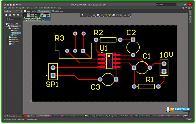
Mainstream Electronic Design Automation (EDA) tools have built-in functionalities to generate the aforementioned manufacturing files, greatly simplifying this process. Common tools include:
- KiCad: A powerful, open-source, and free EDA suite with cross-platform support for Windows, macOS, and Linux. It can easily generate all standard Gerber files, drill files, BOM, pick-and-place files, etc., and has active community support.
- Autodesk EAGLE: Developed by Autodesk, this is a long-standing and widely popular PCB design software that supports scripting capabilities and extensive library resources, suitable for hobbyists and professional users alike.
- EasyEDA / Altium Designer / Cadence Allegro, etc.: EasyEDA is a web-based tool, ideal for beginners and quick prototyping, supporting online file generation and direct ordering on associated platforms (like JLCPCB). Altium Designer and Cadence Allegro are more professional and feature-rich EDA tools, widely used for complex and high-performance PCB designs.
Within these tools, an absolutely crucial step before generating files is to run and ensure a successful Design Rule Check (DRC).

Gerber viewer inspection
3. Checking and Verifying Manufacturing Files: The Final Gatekeeper (Emphasis and Continuation)
Design Rule Check (DRC) – The Pre-Production "Health Check"
Before you click the "Generate Manufacturing Files" button, performing a Design Rule Check (DRC) is a critically important step in the entire PCB design flow; its importance is arguably on par with the design itself. DRC automatically checks your PCB layout against pre-set rules or those obtained from your manufacturer (e.g., minimum trace width, minimum spacing, minimum via size, pad-to-copper clearance, etc.) to ensure it complies with manufacturing process limitations.
- Why is DRC so crucial?
- Ensures Manufacturability: Manufacturers' equipment and processes have physical limitations. For instance, if your trace width or spacing is smaller than their minimum capability, the actual produced boards will likely have short circuits (insufficient spacing causing copper to connect) or open circuits (trace width too thin causing copper to break).
- Avoids Costly Mistakes: Ignoring DRC errors can result in the first batch of prototypes being completely non-functional, leading to a waste of time, money, and materials. Redesigning and re-prototyping significantly delay project timelines.
- Enhances Reliability: Even if a design slightly outside the rules is "luckily" manufactured, its electrical performance and long-term reliability may be compromised, potentially leading to signal integrity issues, thermal problems, or failure under specific environmental conditions.
- What does DRC typically check?
- Clearance: Minimum distance between copper features of different nets.
- Track Width (Trace Width): Minimum and maximum width of conductive traces, set according to current carrying capacity and impedance control requirements.
- Via Size: Drill diameter and annular ring size of vias.
- Pad Size & Spacing: Component pad dimensions, and spacing between pads, and between pads and traces.
- Silkscreen & Solder Mask: Checks if silkscreen overlaps pads (which causes issues during PCB assembly) and if solder mask openings are correct.
- Drill Issues: Whether drills are too close to the board edge, minimum distance between drill holes, etc.
- How to effectively utilize DRC?
- Configure Early, Check Often: Don't wait until the very end of the design to run DRC. Early in the design phase, obtain the recommended design rules from your chosen PCB manufacturer and import or configure them in your EDA tool. Run DRC periodically during the layout and routing process to identify and fix issues promptly.
- Understand and Address Every Error/Warning: Every error or warning in a DRC report deserves careful attention. Analyze its cause: is it a design oversight or an improperly set rule? Some warnings might be acceptable (e.g., intentionally close spacing in a specific area), but you must understand the potential risks.
- DRC is not a panacea, but it's fundamental: Passing DRC doesn't mean the design is perfect (e.g., DRC cannot check for logical errors or performance shortfalls), but it ensures your design is fundamentally manufacturable on a physical level.
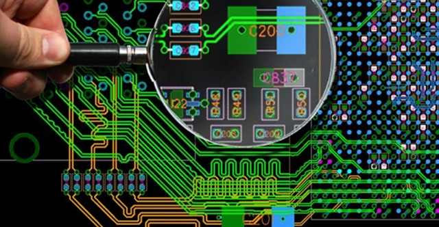
After the DRC passes and you generate the manufacturing files, it is highly recommended to use a standalone Gerber viewer (like Gerbv, ViewMate, GC-Prevue, etc.) for a final manual verification. This acts as a final safeguard for your design:
- Ensure all layers (copper, solder mask, silkscreen, drill, etc.) are generated correctly, can be overlaid without misalignment, and nothing is missing.
- Carefully verify that the drill file's locations, sizes, and quantities match your design.
- Check the silkscreen layer for clear, legible text and component designators, ensuring no overlap with pads or excessively small features.
- Confirm the board outline is correctly closed and its dimensions meet expectations.
- Cross-reference the Gerber files with your original design intent.
Through automated DRC checks and subsequent careful manual verification, you can maximize the chances of identifying and correcting potential manufacturing issues upfront, ensuring your design succeeds on the first attempt and avoiding unnecessary rework and costs.
4. Choosing the Right Manufacturer: Turning Blueprint into Reality
Once you are confident in all your manufacturing files, you can select a suitable manufacturer for both PCB fabrication and PCB assembly. There are many options on the market:
- Elecrow: Offers a one-stop solution from PCB prototyping to small-batch production, component sourcing, and PCB assembly (PCBA) services, also popular for supporting open-source hardware projects.
- J**PCB: Known for its fast turnaround, highly competitive pricing, and convenient online ordering system, ideal for prototyping and small-batch production, including rapid PCB assembly.
- PCBW**: Offers a diverse range of PCB manufacturing services, including standard PCBs, advanced PCBs (like HDI, flexible boards), and comprehensive PCB assembly services, catering to various needs.
- O** Park (USA): Focuses on small-batch, high-quality PCB manufacturing, particularly famous for its signature purple solder mask, popular among hardware enthusiasts abroad, suitable for prototypes with high-quality requirements.
- Numerous other local or international manufacturers: Choose based on your specific needs (e.g., special processes, large volumes, specific certifications).
When selecting a manufacturer, be sure to comprehensively consider their quotes, promised lead times, process capabilities, quality control systems, customer service, and user reviews. Equally important is to fully communicate your design details and any special requirements (such as impedance control for fabrication, or specific soldering profiles for PCB assembly) with the manufacturer.
By following these rigorous steps—from understanding file components, to skillfully using EDA tools and placing high importance on DRC checks, to meticulously verifying files, and prudently selecting a manufacturer—you will be able to confidently transform your well-designed PCB blueprint into a high-quality physical circuit board, laying a solid foundation for your electronic projects.
