Currency
Toggle Nav

Principles and Applications of Online Dual-Sided PCBA AOI (Automatic Optical Inspection) Technology
May 26, 2025
In the current electronics manufacturing landscape, characterized by stringent demands for product miniaturization, high integration, and extreme reliability, the quality control systems for printed circuit board (PCB) manufacturing and subsequent PCB assembly face continuous challenges. The precise placement of every component and the electrical integrity of every solder joint directly determine the performance and long-term reliability of the final electronic product, which is crucial for the entire PCB assembly process. Traditional manual visual inspection methods, with their inherent inefficiencies, subjectivity, and susceptibility to fatigue, can no longer meet the needs of modern precision PCB assembly. Consequently, Automatic Optical Inspection (AOI) technology has become an indispensable key link in the PCB assembly production flow. Among these, online dual-sided PCBA AOI equipment plays a core role in precision manufacturing due to its unique technical principles and significant application advantages. Its technical details and application value, especially in enhancing PCB assembly quality, are worthy of in-depth analysis.
AOI Technology: The Convergence of Optical Imaging and Intelligent Algorithms
Automatic Optical Inspection (AOI) is a technology that utilizes optical imaging principles combined with computer vision and image processing algorithms to achieve automated defect detection. As industry technical literature widely indicates, the core of AOI lies in acquiring high-precision, high-quality optical images and then efficiently and accurately processing this image data, which is crucial for ensuring the quality of the final PCB assembly. Technical exchanges and frequently asked questions within the industry commonly emphasize that AOI systems can effectively identify a variety of surface mount and soldering defects that may occur during the PCB assembly process, including missing components, offsets, incorrect parts, polarity reversals, as well as solder joint issues like too much or too little solder, bridging, and cold solders.
The primary advantages of AOI technology include a significant reduction in labor costs, an increase in the production inspection efficiency of PCB assembly, a unification of inspection standards, and the elimination of inconsistencies in inspection results caused by human factors, thereby ensuring the stability, repeatability, and accuracy of inspections. By promptly detecting and isolating defective products, AOI effectively guarantees the outgoing quality of final products, which is particularly critical for electronic products reliant on high-quality PCB assembly.
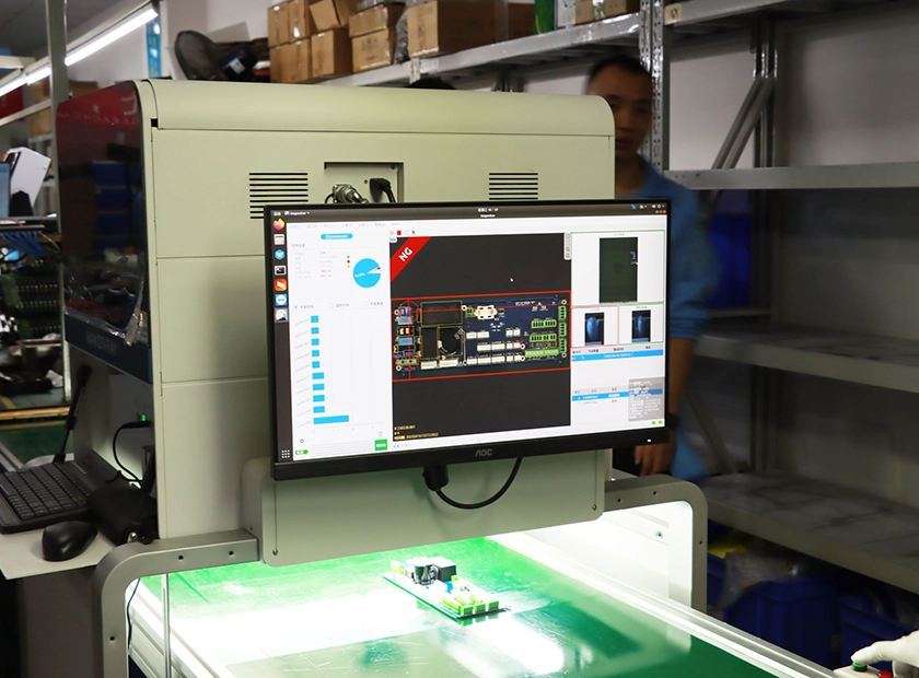
Checking with AOI Device
The "Dual-Sided" Inspection Mechanism: Precision Structure and Workflow of Online Dual-Sided PCBA AOI
With the continuous increase in component packaging density and wiring complexity, dual-sided PCB assembly design has become a common solution for maximizing space utilization. This necessitates inspection equipment capable of comprehensively examining both the top and bottom surfaces of the circuit board, ensuring every stage of PCB assembly is monitored.
The core inspection principle of online dual-sided PCBA AOI equipment is typically based on integrating two independent high-precision optical imaging systems—one upper and one lower—within the device. As the printed circuit board moves through the equipment on an automated conveyor belt during the PCB assembly process, the upper and lower camera modules capture high-speed, high-resolution images of the board's top and bottom surfaces, respectively. This process can be synchronous or asynchronous to optimize inspection cycle times and avoid potential interference between the upper and lower light sources, thereby enhancing the efficiency of the PCB assembly line.
The acquired raw image data is then transmitted to a high-performance image processing unit. At this stage, deep learning algorithms such as Convolutional Neural Networks (CNNs) play a crucial role. By training on a massive number of labeled images of good PCB assembly units and various defect samples, CNNs can automatically extract and learn complex feature patterns that distinguish between good and defective products. During actual inspection, the system compares the real-time captured images with pre-trained models or benchmarks established from known-good boards to intelligently identify component-level defects (e.g., missing parts, incorrect parts, offsets, rotations, tombstones, reverse polarity, damage) and solder joint-level defects (e.g., excessive or insufficient solder, bridging, cold solders, solder balls, lifted leads, open circuits). These are all critical factors affecting PCB assembly quality.
The specific components of the image acquisition system typically include:
- Light Source System: Providing stable, uniform, and adjustable illumination is a prerequisite for acquiring high-quality images, vital for accurately assessing details in PCB assembly. Multi-angle, multi-color (e.g., RGB, white) LED light source combinations are widely used, such as coaxial, ring, low-angle, and dome lights, to highlight different types of defect features.
- Optical Lenses and Cameras: High-resolution industrial cameras, often paired with telecentric or high-depth-of-field lenses, ensure that images are clear with minimal distortion within a specific working distance and field of view (FOV), capable of capturing minute defect details in PCB assembly.
- Levels of Image Processing Algorithms:
- Preprocessing: To provide clearer images for subsequent analysis, forming the foundation for successful defect detection in PCB assembly.
- Feature Extraction and Segmentation: The system must accurately locate the Region of Interest (ROI) for each object being inspected (component or solder joint).
- Defect Classification and Judgment: This is the core intelligence of AOI, directly related to the pass rate of PCB assembly.
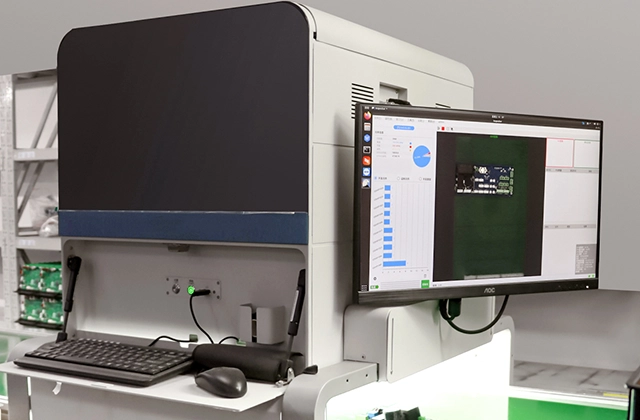
PCBA AOI Device Overview
The Necessity and Value of Dual-Sided AOI in Modern PCBA Manufacturing
- Addressing High-Density and Dual-Sided Layout Challenges: Modern PCB assembly designs are increasingly compact, with dual-sided mounting becoming mainstream. Dual-sided AOI eliminates the need for manual board flipping, completing the inspection of both surfaces in a single pass, ensuring inspection integrity and high efficiency.
- Enhancing Inspection Efficiency and Production Line Throughput: For instance, optimized designs, such as a dual-camera asynchronous image capture, can effectively avoid light source interference, thereby increasing inspection cycle times. This is crucial for high-speed PCB assembly lines.
- Early Defect Interception and Process Control Feedback: Deploying AOI after SMT reflow, DIP wave soldering, or even before packaging allows for the early detection and isolation of defects, whether they originate from early manufacturing stages or deviations during the PCB assembly process. This not only reduces repair costs in subsequent processes but, more importantly, the defect data collected by the AOI system can form a closed-loop feedback mechanism to guide adjustments and optimizations in upstream processes and the PCB assembly flow. This feedback mechanism is a technical guarantee for companies like Elecrow, which are committed to providing a full suite of services from PCB manufacturing and component sourcing to PCB assembly, underpinning their "high-quality PCB assembly service" promise. Their services inevitably include rigorous quality inspection processes, with AOI as an indispensable part, helping them optimize PCB assembly production processes and improve yield rates.
- Data-Driven Management and Traceability: Advanced AOI equipment records detailed inspection data for each inspected board, which is invaluable for tracing issues in the PCB assembly process.
- Overall Cost-Effectiveness: Although the initial investment in AOI equipment is relatively high, its contribution to improving PCB assembly quality and reducing overall costs is significant in the long run.
Deepening AOI Application Scenarios and Exploring Technical Advantages
Typical Application Nodes and Their Inspection Focus:
- After Solder Paste Printing (SPI): Focuses on inspecting solder paste print quality, a critical first step in preventing subsequent PCB assembly soldering defects.
- After SMT Component Placement: Pre-reflow and post-reflow AOI check component placement and solder joint quality, ensuring the reliability of the PCB assembly.
- After DIP Component Wave Soldering: Inspects the soldering of through-hole components, an important part of traditional PCB assembly.
- Final Assembly/Before Packaging (FQA): Serves as the final optical inspection checkpoint before PCB assembly shipment.
Further Interpretation of Key Technical Advantages:
- Programming Convenience and Flexibility: Modern AOI systems support various programming methods, such as CAD data import, simplifying the creation of inspection programs for PCB assembly.
- Detection Rate and False Call Rate: Excellent AOI systems need to strike an optimal balance between these two to ensure the quality and efficiency of PCB assembly.
- Data-Driven Intelligence and Process Improvement: The vast amount of data generated by AOI can be used to optimize the entire PCB assembly process.
- Networking and System Integration (MES/Industry 4.0): AOI equipment can be connected to factory MES for real-time management of PCB assembly data.
Limitations of AOI Technology and Future Development Trends
Although AOI technology is quite mature and widely used, it still has inherent limitations, especially in some complex PCB assembly scenarios:
- Blind Spots for Hidden Defects: For bottom-terminated components like BGAs, standard 2D AOI cannot directly observe them, which can affect the final reliability of the PCB assembly.
- Non-Visual Defects: AOI is primarily based on optical appearance inspection and cannot identify electrical performance defects, requiring other test H_Hethods to fully ensure PCB assembly quality.
Future Outlook:
- Widespread Adoption and Technical Upgrades of 3D AOI: 3D AOI technology can more accurately assess three-dimensional features in PCB assembly, enhancing detection capabilities, which is particularly important for complex PCB assembly.
- Continuous Evolution of AI Algorithms and "Explainable AI (XAI)": Deep learning models will make AOI more intelligent in PCB assembly inspection.
- Multi-Technology Fusion Inspection Solutions (Hybrid Inspection) with AXI, SPI, ICT/FCT: Building integrated intelligent inspection and testing platforms to provide more comprehensive quality assessment for PCB assembly.
- Predictive Maintenance and Intelligent Process Optimization: Proactively adjusting PCB assembly process parameters through long-term trend analysis of AOI and other production line data.
What is more in the future
Online dual-sided PCBA AOI equipment, leveraging its high-precision optical imaging, advanced image processing algorithms, and ever-increasing intelligence, has become a core technology in modern electronics manufacturing processes for ensuring product quality, enhancing production efficiency, and enabling data-driven management. It is crucial for high-quality electronics manufacturing and efficient PCB assembly flows. It is not only a "defect filter" but also a key data source and decision-support tool driving continuous improvement in PCB assembly processes and the upgrade to smart manufacturing. For comprehensive PCBA service providers like Elecrow, whose services span from PCB manufacturing to final PCB assembly, proficiently utilizing and continuously investing in advanced AOI technology is a cornerstone and core competitive advantage in delivering high-quality, high-reliability electronic assembly services, from rapid prototyping to mass production, to their customers. As technology continues to evolve, AOI and its integration with other inspection and testing technologies will play an increasingly critical role in quality control within semiconductor packaging, electronic circuit manufacturing and PCB assembly, and related fields, providing a solid guarantee for the vigorous development of the global electronics industry.