Currency
Toggle Nav

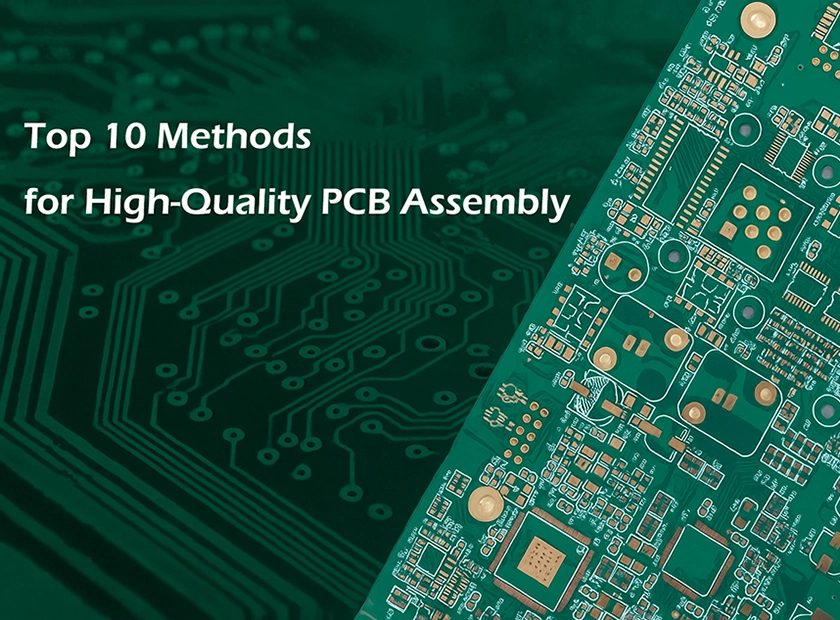
Top 10 Methods for High-Quality PCB Assembly
June 13, 2025
Behind every successful electronic product lies a high-quality circuit board assembly. But the journey from a design file to a perfectly functioning PCBA is fraught with challenges. A single, minute manufacturing defect can lead to total product failure and significant financial loss. How do you build an unbreakable quality firewall? The answer lies in a comprehensive and rigorous testing protocol.
This article will provide an in-depth analysis of the industry's ten most critical testing methods, complete with a comparative table to help you select the most appropriate testing strategy for your project.
Quick Comparison Table of Top 10 Testing Methods
| Testing Method | Primary Purpose | Best For | Pros | Cons |
|---|---|---|---|---|
| AOI | Surface Defect Inspection | Mass Production | Fast, low cost | Cannot detect hidden joints |
| AXI | Internal/Hidden Defect Inspection | Complex components (e.g., BGAs) | High accuracy, broad coverage | Slower, high cost |
| FCT | Full Board Functionality Verification | All finished products | Closest to real-world use | Cannot pinpoint root cause |
| ICT | Comprehensive Electrical Testing | Mass Production | Extremely fast, precise fault location | High fixture cost, inflexible |
| Flying Probe Test | Electrical Performance Testing | Prototypes / Small Batches | No fixture needed, flexible | Slower testing speed |
| Burn-in Test | Screening for Early Failures | High-reliability products | Improves long-term reliability | Time-consuming, high cost |
| Micro-sectioning | Root Cause Analysis | Failure Analysis / R&D | Most precise & visual results | Destructive test |
| Solderability Test | Component Solder-Wetting Verification | Incoming Quality Control (IQC) | Prevents defects at the source | |
| Contamination Test | Ionic Residue Detection | High-reliability products | Prevents long-term failures | |
| TDR Test | High-Speed Signal Impedance Verification | High-frequency PCBs | Ensures signal integrity | Requires specialized equipment |
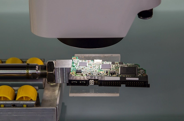
Working Inspection Machine
1. AOI: The Quality Assurance Workhorse of SMT Assembly
Automated Optical Inspection (AOI) is the undisputed quality assurance workhorse in modern SMT assembly processes. It uses high-resolution cameras to rapidly scan a board, comparing its image against a standard "golden board" database to identify component placement and solder joint defects. Modern systems have evolved from basic 2D imaging to advanced 3D AOI, which not only checks for component presence and position but also accurately measures solder paste height, volume, and shape, providing critical data for controlling the crucial solder paste printing process. Strategically placed at key points in the production line, such as post-print and post-reflow, AOI enables the most timely defect capture and process control. This is why professional PCBA service providers like Elecrow consider AOI an indispensable standard procedure, establishing the first line of defense for overall PCB assembly quality.
2. AXI: A Deep Dive into Complex Circuit Board Assembly
If AOI inspects the surface, Automated X-ray Inspection (AXI) performs a 'CT scan' to examine hidden issues within the PCBA. For components like BGAs, where solder joints are completely hidden, AXI uses its penetrative power to clearly visualize their internal state. Advanced 3D AXI systems, employing techniques like laminography, can even virtually slice through a solder ball to precisely identify subtle defects like voids or Head-in-Pillow (HiP) that are difficult for 2D X-ray to detect. Beyond in-line production inspection, AXI is also a powerful tool for Failure Analysis (FA), helping engineers quickly diagnose the root cause of failures in field returns.
3. Functional Test (FCT): Verifying Final PCBA Performance
The Functional Test (FCT) is the 'final exam' of all testing stages, designed to verify if the final PCBA performs according to its design specifications. It no longer focuses on individual components but powers up the entire board to simulate its real-world operating conditions. This process requires a custom test jig that integrates power supplies, signal generators, loads, and necessary communication interfaces. Through a pre-set software script, it sends commands to the PCBA and reads the returned data to determine if its functions meet specifications. The FCT's "Go/No-Go" result is the ultimate judgment on whether a product can be shipped to the customer.
4. In-Circuit Test (ICT): The Efficiency Engine for Mass Production
The In-Circuit Test (ICT) is the ultimate electrical check-up, tailor-made for high-volume circuit board assembly. It uses a custom "bed-of-nails" fixture to make simultaneous contact with all test nodes. To test each component in isolation from its surrounding circuitry, ICT employs a technique called "guarding," which applies specific voltages to adjacent nodes to isolate the component under test. This allows it to accurately measure parameters of nearly all components and locate opens/shorts in seconds. It's important to note, however, that ICT cannot test dynamic interactions between components or the circuit's performance at its actual operating frequency, which is where FCT comes in.
5. Flying Probe Test: Flexible Testing for Prototype PCBAs
The Flying Probe Test is the flexible alternative to ICT, perfectly suited for prototype and small-batch PCBAs. It requires no expensive custom fixtures. Instead, several robotic probes "fly" across the board, contacting test points one by one according to a program. It acts like an automated multimeter, providing R&D engineers with detailed diagnostic reports that pinpoint specific net-to-net issues, which is invaluable for debugging early-stage revisions. Furthermore, flying probe testers are also suitable for designs that lack dedicated ICT test pads, as their probes can directly contact component pads or vias.
6. Burn-In Test
This is a rigorous stress test designed to weed out components within an assembly that are prone to early failure. The failure rate of electronics follows the well-known "bathtub curve," and the purpose of a burn-in test is to get the product past its "infant mortality" phase before it leaves the factory by applying stress far beyond normal operating conditions (e.g., continuous operation at 125°C for tens or hundreds of hours). This test is particularly effective at exposing latent defects within semiconductors, such as micro-cracks, ionic contamination, or poor die bonds. For high-reliability applications, it's a critical value-added service offered by providers like Elecrow for their high-end projects.
7. Micro-sectioning Analysis
This is a destructive, "forensic-level" diagnostic technique used to investigate the root cause of complex issues within a PCBA. A small sample is cut from the board, encapsulated in resin, and then ground and polished to reveal a clear cross-section of its internal structure. This method is the ultimate means of verifying compliance with industry standards like IPC-A-600, allowing engineers to precisely measure copper plating thickness in through-holes, assess the integrity of the lamination structure, and check the registration accuracy of inner-layer pads to the drill hole. It is also often used to evaluate a supplier's process capability or as objective evidence in quality disputes.
8. Solderability Test
This test is typically performed before components are used in circuit board assembly, as part of Incoming Quality Control (IQC). It assesses the ability of component leads and PCB pads to "wet" with solder. Common methods include the "Dip and Look" test and the more precise "Wetting Balance" method, which quantifies the change in wetting force over time during soldering. Neglecting solderability testing can have catastrophic consequences, especially for components that have been in storage for a long time or are from questionable sources, potentially leading to hard-to-repair soldering defects in mass production.
9. Contamination Test
After assembly, invisible ionic residues on the board's surface, such as flux or perspiration, can become a "ticking time bomb." When combined with ambient moisture, these contaminants can trigger "electrochemical migration," causing tiny metallic dendrites to grow between electrodes, eventually leading to short circuits. To detect these risks, the industry commonly uses the ROSE (Resistivity of Solvent Extract) test for a quick assessment of overall ionic cleanliness, or the more precise Ion Chromatography (IC) to analyze the type and concentration of specific contaminants. The test results directly validate the effectiveness of the cleaning process, ensuring that "no-clean" flux residues are truly benign.
10. TDR / Impedance Control Test
This test is specifically for PCBAs that incorporate high-speed circuits. In high-speed signal transmission, the "characteristic impedance" of a trace must be extremely precise and uniform; otherwise, signals will suffer from reflections and distortion due to impedance mismatches. The root causes of these mismatches are often minute variations in trace width/thickness, improperly designed vias, or the transition area between a connector and the PCB. A Time-Domain Reflectometer (TDR) acts like radar, sending a nanosecond-level pulse down a trace and analyzing its echo. It is a critical tool for verifying that the PCB manufacturer has strictly adhered to the design's impedance control requirements, bridging the gap between design simulation and physical reality.
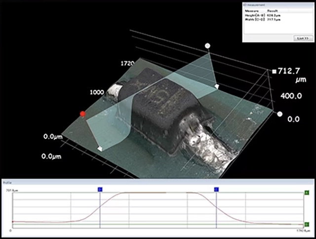
PCB Failure Analysis and PCB Defect Analysis
How to Choose the Right Testing Strategy for Your Project
After understanding these ten methods, the most critical step is to tailor an effective testing strategy to your project's specific circumstances. This is not a simple choice but a decision-making process that requires a comprehensive consideration of cost, risk, and time-to-market.
For Prototypes and Small Batches: Focus on Debugging and Rapid Iteration
In the early stages of a project, the primary goals are rapid design validation and iteration. The testing strategy's core should be flexibility and diagnostic capability, rather than striving for 100% automated coverage. The recommended combination is a Flying Probe Test + AOI + Manual Functional Verification by Engineers. The flying probe test, with its lack of expensive custom fixtures, can quickly adapt to design changes and provide engineers with precise electrical fault diagnostics. AOI serves as a basic safeguard, quickly eliminating obvious assembly errors. Finally, functional verification performed by the engineers who know the design best can uncover logic and performance issues that automated scripts might miss.
For Mass Production: Focus on Efficiency, Consistency, and Process Control
Once a product's design is finalized and enters mass production, the focus of testing shifts to efficiency, cost control, and quality consistency. The gold standard here is an automated line featuring AOI + ICT + FCT. AOI and ICT form a powerful "manufacturing defect filter," with AOI catching all visually apparent errors and ICT performing comprehensive electrical checks at high speed. They serve not only as screening tools but also as data sources for Statistical Process Control (SPC). FCT then acts as the final "customer experience simulator," ensuring that every PCBA that passes through the preceding stages works perfectly as a system, thereby maximizing First Pass Yield (FPY) and reducing rework costs.
For High-Reliability Products: Focus on Risk Mitigation and Long-Term Stability
For mission-critical applications in sectors like medical, automotive, or aerospace, the testing strategy starts from a premise of zero-defect tolerance and long-term reliability under extreme conditions. Cost becomes a secondary consideration to risk mitigation. In addition to the standard mass-production tests, deeper levels of inspection are required. AXI becomes mandatory to ensure the integrity of internal solder joints in complex packages. Burn-in Testing proactively screens out products at risk of early failure by simulating extreme operating conditions. Contamination Testing ensures that no chemical residues will cause corrosion or shorts in the years to come, fulfilling stringent industry certification requirements.
Ultimately, the best testing strategy is not an isolated checklist but the product of deep collaboration between you and your manufacturing partner. An excellent Electronic Manufacturing Services (EMS) partner like Elecrow will not only execute the tests you request but will also provide Design for Testability (DfT) advice during the design phase. This collaboration helps you optimize your design for testing, fundamentally reducing future manufacturing costs and quality risks, and achieving the perfect balance between quality, cost, and time-to-market to ensure your project's success.