Currency
Toggle Nav

Understanding and Preventing Solder Bridges in PCB Design
May 16, 2025
In the intricate world of precision electronics, a seemingly insignificant flaw can often trigger a cascade of issues, potentially leading to complete system failure. The "solder bridge" is precisely such a covert "saboteur" lurking within circuit boards. For any electronics engineer or product developer, witnessing a meticulously designed circuit board ultimately fail due to an inadvertent soldering error is undoubtedly frustrating and can be exceptionally costly. Therefore, a thorough investigation into the causes of solder bridges, a clear understanding of their detrimental effects, and a mastery of preventative strategies spanning the entire lifecycle—from design through manufacturing to assembly—are of paramount importance.
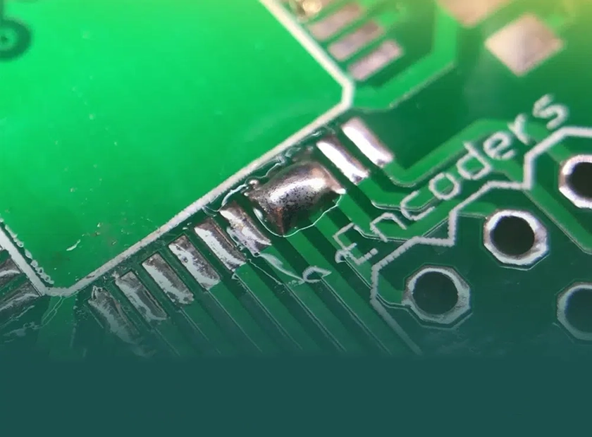
Typical Solder Bridge
To effectively address solder bridges, we must first clearly understand what they are. Here’s a very incisive description: "A solder bridge forms when two points on a circuit board that are not designed to be electrically connected are inadvertently connected by solder over the top of the PCB solder mask. This creates an electrical short that can wreak all kinds of havoc, depending on what the two points that are shorted together are designed to do." This statement highlights the essence of a solder bridge—the formation of an unintended conductive path on the circuit board. The consequences of such a short circuit can vary widely, from causing minor equipment malfunctions and significant performance degradation to, in severe cases, burning out critical components or even posing safety hazards like overheating or smoke. Its potential for "havoc" should not be underestimated.
So, where do these troublesome solder bridges originate? Their formation is often the result of multiple intertwined factors. As experience in the field has shown: "Solder bridges can be caused by a lot of things, ranging from bad solder paste stencils or bad placement registration to messy assembly lines or clumsy rework techs." Specifically, key contributing factors include:
- Process Materials and Initial Setup:
- Poor quality or improperly designed solder paste stencils (e.g., issues with apertures, thickness, or flatness) leading to excessive or misplaced solder paste deposition.
- Non-compliant physicochemical properties of the solder paste itself (e.g., viscosity, metal content, particle size) causing abnormal behavior during soldering.
- Equipment Precision and Operational Standards:
- Poor component placement registration, resulting in insufficient clearance between component leads and adjacent pads or leads.
- Improper settings for solder paste printing parameters (e.g., squeegee pressure, printing speed, snap-off distance) affecting the solder paste deposit profile.
- Production Environment and Operator Skill:
- Contaminated production lines (e.g., with dust or foreign particles) increasing the risk of pad or solder paste contamination, affecting solder wetting and flow.
- Non-standard rework techniques, especially during manual soldering (e.g., excessive solder dragging, improper heating time control, or insufficient skill).
Delving deeper, the physical properties of solder itself play a subtle yet crucial role. We must understand that: "Solder naturally wants to wick towards heated metal or other melted solder, and a lot of the printed circuit board assembly process relies on that fact. When solder reflows, it has a lot of surface tension, so it tends to stay balled up where it belongs and to hold things to it, nicely. Anything that disrupts that natural tendency can lead to bridging." This statement profoundly points to the core of the issue. It implies that if the circuit board design itself has flaws, such as excessively small pad-to-pad spacing or overly large solder mask openings, or if the board experiences uneven heating or too rapid a temperature rise during reflow soldering, the natural surface tension balance and cohesive forces of the solder can be disrupted. This can cause the solder to "lose control" and spread, ultimately forming bridges in unintended locations.

PCB close-up Macro PCB
Given such complex etiologies, comprehensive, full-lifecycle prevention measures become particularly crucial. Professional electronics manufacturing service providers, leveraging their profound technical expertise and stringent quality control systems in PCB manufacturing and PCB assembly, can offer one-stop solutions to systematically mitigate solder bridge risks.
During the PCB manufacturing stage, a high-quality bare board is the foundational defense. Key preventative measures at this stage include:
- Employing precise solder mask application processes to ensure its integrity, uniformity, and registration accuracy, effectively confining solder to the target pads.
- Utilizing advanced etching and imaging technologies to guarantee that pad dimensions, shapes, and spacing strictly adhere to design specifications; sensible pad design (e.g., using "solder mask dams" between fine-pitch leads) also cleverly utilizes solder's surface tension.
- Conducting a 100% electrical test before bare board shipment to preemptively identify potential open and short circuit hazards introduced during manufacturing.
- Selecting an appropriate surface finish, such as HASL (Hot Air Solder Leveling), ENIG (Electroless Nickel Immersion Gold), or OSP (Organic Solderability Preservatives), to ensure good solderability of the pads, promoting uniform solder wetting and preventing solder buildup due to poor wetting.
Moving into the PCB assembly stage, meticulous process control is central to avoiding solder bridges. Reputable assembly service providers will focus on:
- Solder Paste Printing: Precisely fabricating laser-cut stencils based on design files and utilizing high-precision printing equipment to ensure optimal solder paste volume and position.
- Component Placement: Using high-precision pick-and-place machines to accurately position components at the center of their pads, preventing excessively close lead spacing due to positional deviation.
- Reflow Soldering: Meticulously designing and optimizing the reflow temperature profile based on PCB material, thickness, and component types, ensuring solder melts, wets, flows, and solidifies under ideal conditions.
- Process Standardization and Cleanliness: Strictly adhering to standardized process flows and maintaining production line cleanliness.
- Manual Operations: Ensuring professional handling of manual soldering or rework by skilled technicians.
- Advanced Inspection: Employing methods like Automated Optical Inspection (AOI) and X-Ray inspection (for BGAs, QFNs, etc.) for comprehensive examination of post-soldering PCBAs.
Of course, the effort to prevent solder bridges does not solely begin at the manufacturing and assembly stages. Design engineers should adopt a forward-thinking approach from the initial circuit board design phase, fully considering Design for Manufacturability (DFM) principles. This includes:
- Setting reasonable pad spacing and dimensions.
- Correctly using solder mask dams between fine-pitch component leads as physical barriers.
- Avoiding direct connections of large copper areas to small pads, to prevent uneven heat dissipation that could affect soldering quality.
So, while solder bridges may seem like a minor issue in the electronics manufacturing process, their potential harm should not be underestimated. They are not only a direct test of manufacturing and assembly process capabilities but also place higher demands on front-end design philosophies. Only by deeply understanding their causes and by according high importance and strict control at every stage—from design, through PCB manufacturing, to PCB assembly—can this "silent saboteur" be effectively kept at bay. Opting for professional partners who can provide one-stop services, encompassing PCB design support, high-quality PCB manufacturing, and precision PCB assembly, is undoubtedly a wise choice to ensure the success of your electronic product projects. With their professional technical capabilities, advanced production equipment, and robust quality control systems, they can help you maximally mitigate solder bridge risks throughout the complex electronics manufacturing process, ensuring the stability and reliability of your final products. If you are seeking reliable solutions for solder bridge issues or other manufacturing and assembly challenges for your circuit boards, thoroughly investigating and selecting service providers with extensive experience and a strong reputation in PCB manufacturing and PCB assembly will be a critical step towards success.