Currency
 Back to School with STEM-Limited-Time Event(Aug 6-Sep 5)
Back to School with STEM-Limited-Time Event(Aug 6-Sep 5)

Printed Circuit Boards (PCBs) are the foundational backbone of modern electronics, providing a platform to mount components and create the electrical connections that bring devices to life. A PCB is not a single entity but a complex sandwich of different materials and layers, each with a specific function. While designers and engineers talk about signal layers, power planes, and substrates, the term "assembly layer" can be a point of confusion.
So, what exactly is the assembly layer of a PCB?
In short, there is no single, official layer called the "assembly layer." Instead, it is a functional concept referring to a group of layers that work together to guide the manufacturing process of placing (assembling) and soldering components onto the board. These layers provide the critical information needed for both automated machinery and human technicians to ensure a correct, efficient, and reliable pcb assembly.
Let's break down the key layers that constitute this "assembly system."
These layers are directly created and used to facilitate the PCB assembly process.
The silkscreen, also known as the overlay, is arguably the most recognizable assembly-related layer. It is a layer of ink (typically white, black, or yellow) printed onto the top and/or bottom surfaces of the PCB.
Function: Its primary purpose is to provide human-readable information. This includes:
R1, C5, U2 to identify which component goes where.The silkscreen layer is the essential visual guide for manual assembly, testing, and debugging. It explains the board's layout and the function of its components at a glance.
This layer is indispensable for modern Surface Mount Technology (SMT) assembly. It's not a physical layer on the finished PCB but a digital template used during manufacturing.
Function: The solder paste layer defines precisely where solder paste should be applied to the board. In an automated assembly line, a stencil based on this layer's design is laid over the PCB. Solder paste is then squeegeed through the openings in the stencil, depositing it only on the component pads. The surface tension of this paste temporarily holds the SMT components in place before the entire board goes through a reflow oven to melt the solder and create permanent connections.
Without the solder paste layer, precise and repeatable SMT assembly would be impossible.
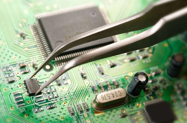
SMT pads on a circuit board
The solder mask is the thin, protective polymer coating that gives most PCBs their characteristic green color (though other colors are available). While its main role is protection, it is fundamentally crucial for assembly.
Function in Assembly: The solder mask covers all the copper traces on the board except for the pads where components are meant to be soldered. By selectively exposing these pads, the solder mask:
In essence, the solder mask defines the "solderable" areas, making it a critical guide for the soldering process.
Applied on top of the exposed copper pads (the areas not covered by the solder mask), the surface finish is a very thin metallic or organic coating.
Function in Assembly: Its primary role is to protect the copper pads from oxidation and to provide a clean, solderable surface. A bare copper pad would quickly oxidize, making it difficult to solder to. Common surface finishes like HASL, ENIG, and OSP ensure that when the board is assembled, the solder can form a strong, reliable intermetallic bond with the pads. This is vital for the quality and longevity of the final product.
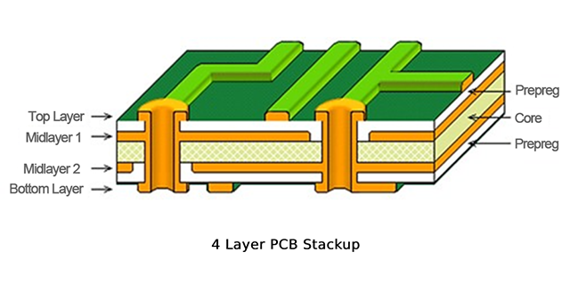
4-layer-PCB-stackup
While the layers above are directly for assembly, other fundamental PCB layers provide the physical foundation for it.
Understanding how PCBs are made clarifies the role of assembly layers.
The "assembly layer" of a PCB is not a single layer but a system of functional layers—primarily the Silkscreen, Solder Paste, Solder Mask, and Surface Finish layers. They do not carry electrical signals but serve a more critical manufacturing role: they provide a comprehensive set of instructions for building the circuit. They guide where components go, where solder should be applied, what to protect, and what to leave exposed. A deep understanding of these layers is essential for a successful pcb assembly, leading to a reliable and functional electronic device.