Currency
Toggle Nav

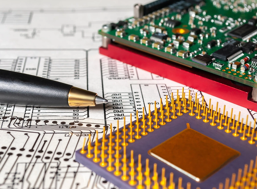
A Complete Guide From KiCad Design to PCB Prototyping Order
May 27, 2025
This tutorial is aimed at users who have already completed their circuit design in KiCad. It focuses on how to correctly export design files and place a prototype order with Elecrow. We assume you are familiar with basic KiCad operations, including schematic capture, footprint assignment, and PCB layout.
Elecrow's official website usually provides its own recommended Gerber export parameter settings, which you can also refer to.
Check your Final Design at first (very important)
1. DRC (Design Rule Check)
- Before exporting manufacturing files, always run KiCad's DRC function.
- Fix all reported errors. Even 'Warning' level messages should be individually assessed. Ignoring DRC errors can lead to PCB manufacturing failures or functional issues.
- KiCad's default DRC rules are suitable for general designs. For special process requirements, adjust them according to the rules provided by the PCB manufacturer (like Elecrow).
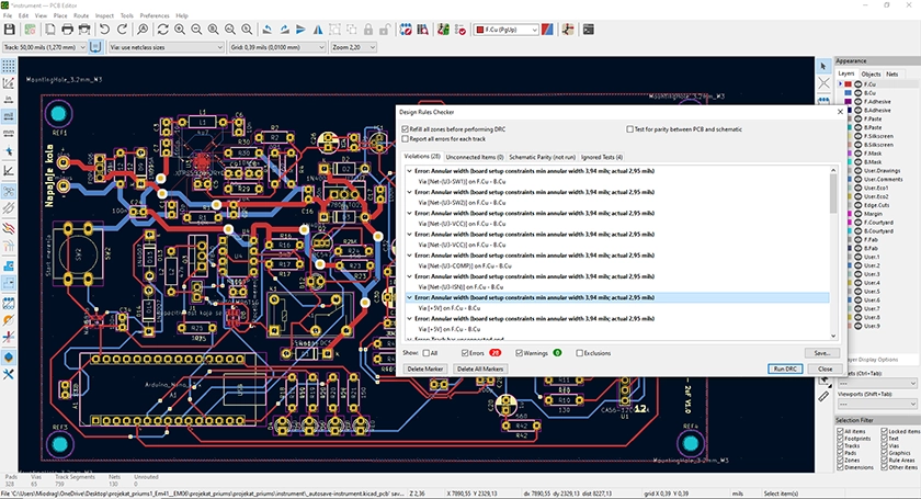
1. Run DRC on KiCad after you have finished design
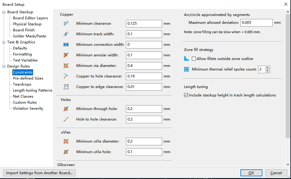
Elecrow Design Rules 1
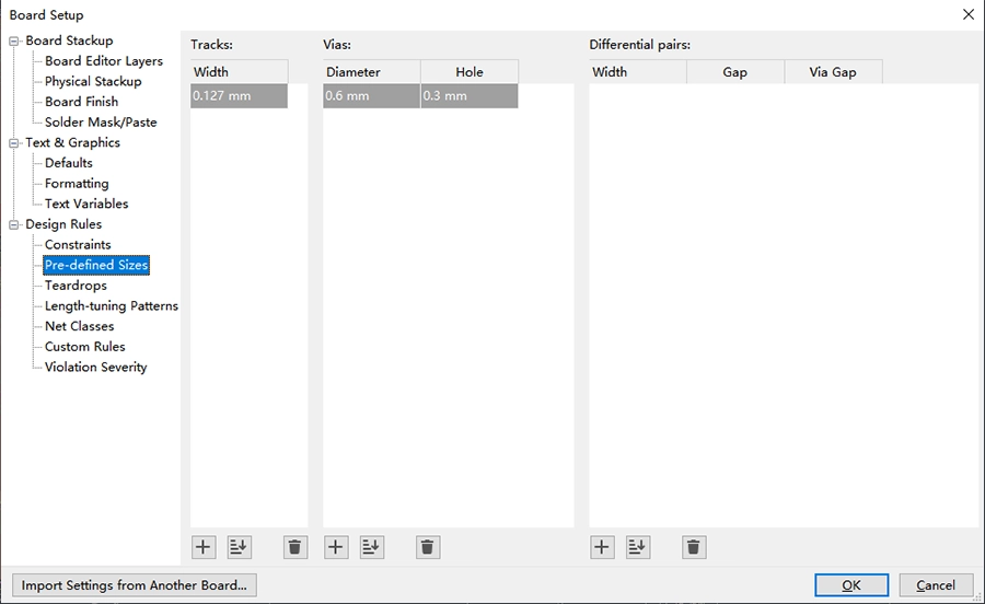
Elecrow Design Rules 2
2. 3D Preview Check (Recommended)
- Use KiCad's built-in 3D viewer to quickly check for potential issues such as:
- Incorrect or misplaced component footprints.
- Overlapping silkscreen text or text over pads/traces.
- Incorrect connector orientation.
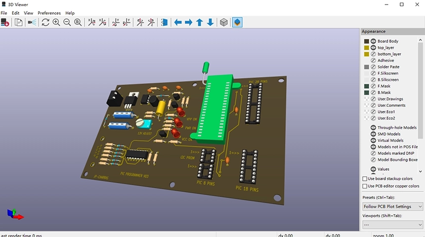
2. KiCad 3D Viewer
3. Pad Size and Critical Mechanical Dimension Check
- Verify that pad sizes conform to component specifications, especially for SMD (Surface Mount Device) components.
- Measure critical interface dimensions (e.g., USB ports, mounting holes) to ensure they meet mechanical assembly requirements.
- Ensure the board outline on the
Edge.Cutslayer is complete and closed, as this will be used for PCB routing (cutting).
Generating Manufacturing Files (Gerber & Drill Files)
1. Gerber File Export
In the KiCad PCB Editor (Pcbnew), use File > Plot.
- Output directory: It's recommended to create a separate output directory (e.g.,
gerberorproduction) within your project folder to store these files. - Include layers (Essential):
F.Cu(Front Copper / Top Copper)B.Cu(Back Copper / Bottom Copper)F.Mask/B.Mask(Front/Back Solder Mask)F.SilkS/B.SilkS(Front/Back Silkscreen)Edge.Cuts(Board Outline)- (Depending on your design, you might also need
F.Paste/B.Pastefor SMT stencils, but the above are core for PCB fabrication.)
- Recommended Settings (Gerber Options & General Options):
- Plot format: Gerber
- Coordinate format: KiCad's default (e.g., 4.6 for metric, or 2.5 for imperial) is usually recommended. Ensure units match your design.
- Check "Use Protel filename extensions" (recommended by many manufacturers for easy layer identification).
- Check "Subtract soldermask from silkscreen" (prevents silkscreen from being printed on solder pads).
- The "Use auxiliary axis" option should generally be left unchecked (default) unless you have specifically defined an auxiliary origin.
- Output units: Select mm or inches, consistent with your design and subsequent order placement.
2. Drill File Export
In the Plot dialog, click "Generate Drill Files...":
- Output Directory: Ensure it's the same as the Gerber output directory.
- Drill File Format: Excellon
- Drill Units: Select mm or inches, consistent with Gerber settings and your design.
- Drill Origin: Typically Absolute.
- Zeros Format: KiCad default or manufacturer's recommendation (e.g., Suppress leading zeros, or Decimal format).
- Ensure all drill information (including PTH - Plated Through Holes and NPTH - Non-Plated Through Holes) is included. KiCad usually merges them into one
.drlfile. If separate NPTH files (e.g.,*-NPTH.drl) are generated, include them in the package. - Checking "Generate Map File" is optional but can aid later inspection.
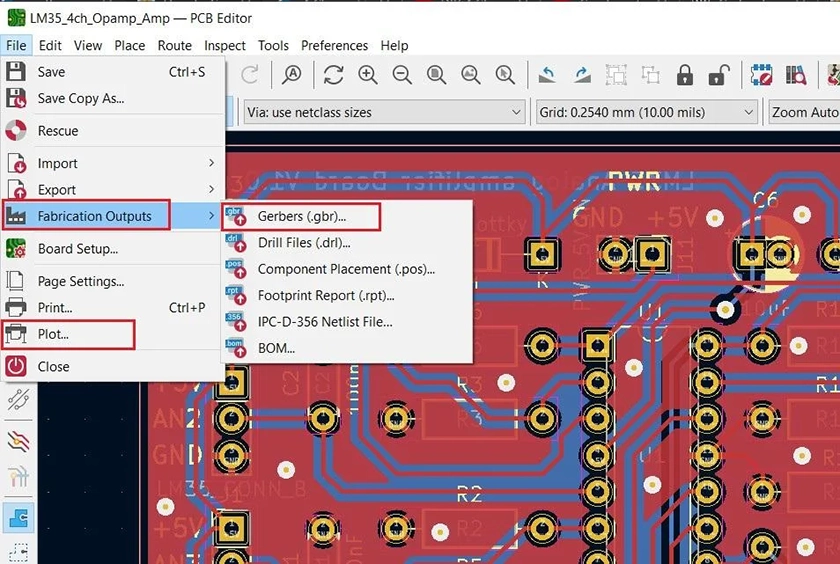
3. Fabrication Outputs Gerber Files and Drill Files
3. Package into a Zip Archive
Package all generated Gerber files and Drill files into a single .zip archive. Typically, it should include (Protel extension examples):
*.GTL(Top Copper Layer)*.GBL(Bottom Copper Layer)*.GTS(Top Solder Mask)*.GBS(Bottom Solder Mask)*.GTO(Top Silkscreen)*.GBO(Bottom Silkscreen)*.GKOor*.GMx(Board Outline / Mechanical Layer, corresponding toEdge.Cuts. The specific extension might vary based on KiCad version/settings).*.DRL(Drill file)- Possibly
*-NPTH.DRLif NPTH drills were not merged. - Possibly
*.GTP(Top Paste),*.GBP(Bottom Paste) if stencil files are included.
Placing a PCB Prototype Order on Elecrow
1. Register & Login
- Visit Elecrow's official website, register for an account, and log in.
2. Navigate to the Order Page
- Click on "PCB Prototyping," "Quick Order," or a similar link on the homepage to access their online quoting system.
3. Upload Gerber Archive
- Upload the
.zipfile you created. The system will usually attempt to auto-detect the layers. If there are any recognition issues, you may need to manually assign the file type for each layer.
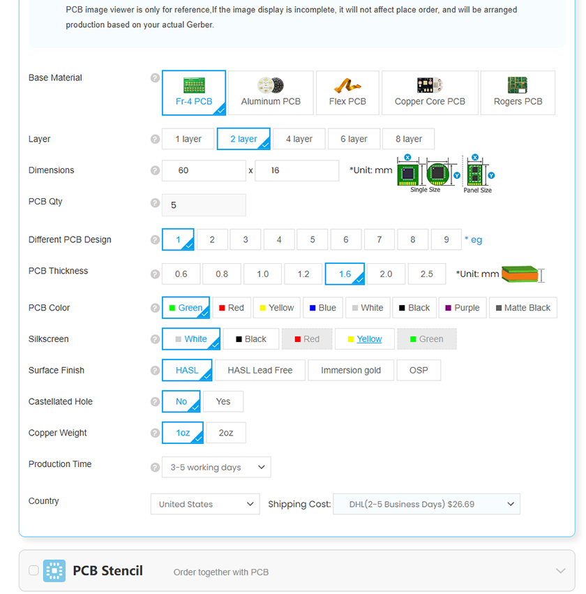
4. Configure Manufacturing Parameters (Core Step)
| Parameter | Description | Beginner Recommendation |
|---|---|---|
| Layers | Common options are 2 or 4 layers. | 2 Layers |
| Material | Default is FR-4. | FR-4 |
| Thickness | Common value is 1.6mm. | 1.6mm |
| Copper Weight | Copper thickness per side, in oz. | 1 oz |
| Solder Mask Color | Green is standard. | Green |
| Silkscreen Color | Usually white. | White |
| Surface Finish | HASL is economical; ENIG for finer features. | Lead-Free HASL |
| Quantity | Minimum order quantity (MOQ) is often 5 pcs. | 5 pcs (or as needed) |
| Special Process | E.g., blind/buried vias, gold fingers. | Avoid unless required |
ENIG (Electroless Nickel Immersion Gold) surface finish is suitable for fine-pitch BGAs and other demanding applications but is more expensive.
5. Gerber Online Preview
Elecrow (and many other fabs) provide an online Gerber viewer. It is crucial to thoroughly review this preview:
- Confirm dimensions are correct, especially checking units (mm/inch).
- Verify that drill holes align correctly with pads.
- Ensure silkscreen is not printed over pads/traces or extends beyond the PCB boundary.
- Check that all layers display as expected.
- Pick the services you want.
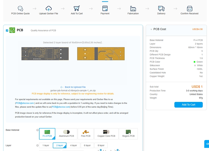
4. Gerber online preview
5. Pick the services
6. Submit Order & Payment
- Confirm the final price, fill in your shipping information, and complete the payment. PayPal or international credit cards are commonly supported.

6. Check the list and add to cart and pay
Post-Receipt PCB Inspection (Recommended)
After receiving the PCBs from Elecrow, it's recommended to perform the following checks:
- Overall Dimensions: Check if they match your design and look for any burrs or warping.
- Silkscreen Clarity: Ensure the font is legible and there's no misalignment.
- Drill Hole Alignment: Confirm holes are accurately centered on their respective pads.
- Solder Mask Alignment: Verify that the solder mask does not cover solderable pads.
- Board Quantity: Ensure the quantity received matches your order.
You can use calipers and a multimeter to further verify electrical characteristics and critical mechanical dimensions.
If you find any significant issues, take clear photos and contact Elecrow customer service for assistance.
Focusing on the Core Prototyping Process
This tutorial bypasses basic KiCad introductory content, focusing on the key steps from design completion to prototype ordering. It's suitable for users with some existing KiCad knowledge to quickly get their designs manufactured.
- Thoroughly check design rules and critical dimensions.
- Correctly export Gerber and drill files.
- Accurately configure Elecrow order parameters.
- Promptly inspect the physical boards upon receipt.
Mastering these steps will allow you to confidently take your KiCad designs to production, successfully making the first step from digital design to physical realization.