Currency
 Back to School with STEM-Limited-Time Event(Aug 6-Sep 5)
Back to School with STEM-Limited-Time Event(Aug 6-Sep 5)
Micro:bit is an ARM-based embedded system designed by the BBC for use in computer education in the UK. The BBC gave away the computer free to every year 7 child in Britain starting from October 2015(around 1 million devices). Micro:bit now becomes a worldwide popular device. The Micro:bit Foundation aims to put the device into the hands of 2 million children in the U.S. & Canada by 2020. "The goal of the micro:bit is to give educators and parents an easy-to-use tool to teach the basics of computer programming and inspire students to imagine, invent and innovate." said Hal Speed, Head of North America at the Micro:bit Foundation. In Japan, the Micro:bit Foundation's goal is to deliver the micro:bit to 300,000 Japanese children by 2020. In Croatia,
All the electronic products have to use PCB to function, so there is a consensus that the trend of PCB market almost indicates the dynamic of the electronic industry. With the development of phone, laptop and PDA and the other advanced, small-sized electronic products like the wearable devices, the demands for flexible printed circuit boards are increasingly growing. PCB manufacturers are focused to create thinner, lighter and higher-density FPC to seize this thriving market. Under the background, I consider it necessary to write about the differences between single-sided flex PCB, double-sided flex PCB and multilayer flex PCB, whether for the PCB fabricators or the open source hardware makers who are likely to buy
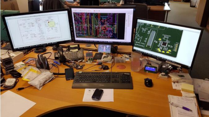
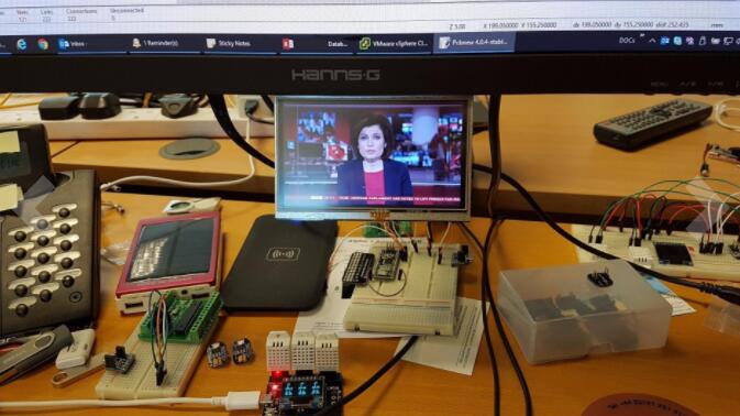
Raspberry Pi touch Screen monitor is widely used by the Raspberry Pi fans. They can make Raspberry Pi tablet, game console, TV display with the Raspberry Pi touch screen.
Raspberry Pi touch screen is one of the hottest items on Elecrow product list, no matter it's on our own store or on Amazon. Let's see what customers used it for and what's their experiences.
Watch TV on Raspberry Pi Screen(Display)
When a PCB layout and routing is completed and both the connectivity and spacing are inspected without faults, does it mean the PCB design is succeeded and finished? Of course no. A final inspection is often ignored or neglected by some new engineers, this is likely to result in some bugs or problems in prototyping or even re-prototyping, such as the sockets getting too close, or loop signal and so on. Therefore, a final inspection is a must-do thing of PCB layout. A good final inspection process involves lots of specific steps, here listed some steps that I found quite important but easy to be ignored. 1.Footprint 1). Pads spacing. For the new components, it’s necessary
Christmas is the most important festival for many people. As a maker or electronic engineer, how can we celebrate Christmas in our own special way? Before Christmas 2016, we held a Christmas PCB Contest in Elecrow facebook group, there were several fascinating projects. As we did before, Elecrow provided
1. The overlap of the welding plates. a. The overlap of welding plates means the holes are overlapped, when multiple drilling happens to one position, it would result in the damage of hole. b. Overlap of two holes in a multi-layer board will cause it scrapped. 2. The abuse of graphics layer. a. Doing some useless connection in the graphics layer is easily misunderstood, for example, a design for 4 layer PCB uses the circuit of 5 layer PCB or even above. b. In violation of conventional design, such as, the side of electronic parts is designed at the Bottom layer, and the welding side is designed at the Top layer, these all will cause troubles. 3. The characters are in a mess.
The basic principle for the whole process of PCB design is: make the whole design beautiful as much as possible on the basis of following the requirements of product electrical and mechanical structure, keep the layout of electronic parts uniform and orderly in the printed circuit board. Here are the items and tips you should check:
Panelizing is common used in the PCB board’s production for it can get more value in a low cost. For some customers, the size of single boards can’t properly used on their project so they need a bigger size. That’s the main reason for customer choose panelizing service, here is an introduction of panelizing service of Elecrow. We have two ways of panelizing, one is V-cut and the other is snap off holes. For V-cut, the minimum size of board is 8*8cm. V-cut is a straight and uninterrupted line, the mini spacing between 2 V-cut line is 2mm, and different thickness has different request. For 1.6mm thickness boards, V-cut line must has 1mm spacing with the edge of boards; for 1.0mm thickness should be 0.7mm. Customer can add the V-cut line in the GKO layer or the silkscreen