Currency
Toggle Nav

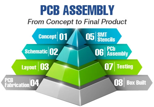
What is a Turnkey PCB Assembly Process?
September 15, 2025
Understanding the Foundation of All Modern Electronics
Every electronic device, from a simple digital watch to a complex supercomputer, relies on a Printed Circuit Board Assembly (PCBA). While many people have heard of a Printed Circuit Board (PCB), the term PCB assembly refers to the critical manufacturing process that transforms a bare board into a fully functional electronic circuit. Without this process, our digital world would not exist.
This definitive guide provides a comprehensive overview of PCB assembly. We will break down the terminology, detail every step of the manufacturing process, explore the different types of assembly services available, and offer practical advice on how to select a high-quality pcb assembly service. This article is designed to be the only resource you need to fully understand the world of PCBA, whether you are an engineer, a business owner launching a new product, or simply curious about how electronics are made.
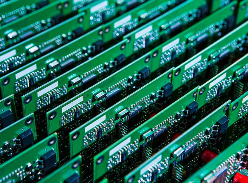
Foundation of All Modern Electronics
Section 1: Foundational Terminology in PCB Manufacturing
To understand the assembly process, we must first be clear on the key terms. Misunderstanding these can lead to costly errors when communicating with a pcb assembly manufacturer.
- PCB (Printed Circuit Board): This is the flat, bare board, typically made from fiberglass (like FR-4). It contains a pre-designed layout of copper pathways, or "traces," that connect different points. A bare PCB is an inactive component; it is the foundation, but it performs no electronic function on its own.
- PCBA (Printed Circuit Board Assembly): This is the final, populated board. A PCBA is a PCB that has undergone the PCB assembly process, where all the necessary electronic components (like integrated circuits, resistors, capacitors) have been mounted and soldered onto it. This is the active, functional heart of an electronic device.
- Electronic Components: These are the individual electronic parts that are mounted onto the PCB. They range from tiny resistors to complex microprocessors.
- Soldering: The process of joining the electronic components to the copper traces on the PCB using a metal alloy called solder, which melts to form a strong electrical and mechanical bond.
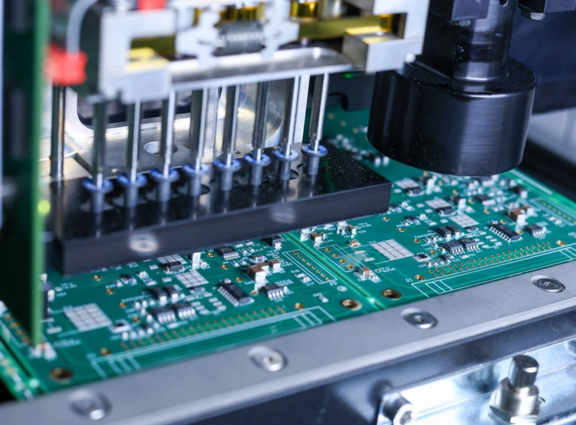
Pcb Assembly All Steps Overview
The Crucial Distinction: PCB Fabrication vs. PCB Assembly
A common point of confusion is the difference between "fabrication" and "assembly." They are two distinct, sequential stages of the overall pcb manufacturing and assembly process.
- PCB Fabrication: This is the creation of the bare board itself. It involves processes like etching the copper traces, drilling holes (vias and pads), and applying the solder mask (the green, blue, or red protective layer).
- PCB Assembly: This is the process of taking a fabricated bare board and mounting all the electronic components onto it.
Many companies offer both services as a single, integrated solution, often referred to as "pcb fabrication and assembly," to ensure a seamless workflow from design to the final functional product.
Section 2: The Detailed, Step-by-Step PCB Assembly Process
The modern PCB assembly process is a highly precise and largely automated sequence. While variations exist, the core steps performed by any professional pcb assembly manufacturer are as follows:
- Step 1: DFM/DFA Check (Design for Manufacturability/Assembly)
Before any physical production begins, engineers review the client's design files (Gerber files, Bill of Materials). This crucial check ensures that the design is not only functional but also optimized for efficient and error-free manufacturing. - Step 2: Solder Paste Application
For surface-mount components, a solder paste (a mixture of tiny solder particles and flux) is applied to the component pads on the PCB. A thin, stainless-steel stencil is placed over the board, and a squeegee blade presses the paste through the stencil's apertures, ensuring a precise amount of paste is deposited in the exact right locations. - Step 3: Automated Component Placement (Pick-and-Place)
This is the core of SMT PCB assembly (Surface-Mount Technology). A robotic machine called a Pick-and-Place uses vacuum nozzles to pick up electronic components from reels and trays and places them onto the solder paste on the PCB with incredible speed and precision. - Step 4: Reflow Soldering
Once all surface-mount components are placed, the board is moved through a long industrial oven called a reflow oven. The board travels through multiple zones with controlled temperatures that carefully heat the board to melt the solder paste, forming permanent solder joints. It is then cooled in a controlled manner to solidify these connections. - Step 5: Post-Reflow Inspection (AOI & X-Ray)
Quality control is critical. After reflow, the boards are inspected for defects.- Automated Optical Inspection (AOI): A machine uses high-resolution cameras to scan the board and compare it to the design, checking for issues like incorrect components, missing parts, or poor solder joints.
- X-ray Inspection: For components like BGAs (Ball Grid Arrays) where the solder joints are hidden underneath the chip, an X-ray machine is used to see through the component and verify the quality of the connections.
- Step 6: Through-Hole Component Insertion
If the design includes Through-Hole Technology (THT) components (like large connectors or capacitors with long leads), they are inserted at this stage. This can be done by a skilled technician, known as a pcb assembler, or by automated insertion machines. - Step 7: Wave or Selective Soldering
For THT components, the board is passed over a wave of molten solder (wave soldering) that solders all the leads at once. For boards with mixed technology, a more precise method called selective soldering may be used to target only the through-hole pins without disturbing the already-soldered surface-mount parts. - Step 8: Final Inspection and Functional Testing
After all soldering is complete, the board undergoes a final visual inspection and, most importantly, a functional test. This test powers up the PCBA and simulates its real-world operation to confirm it functions exactly as designed. A thorough pcb fabrication and assembly process always concludes with rigorous testing.
Section 3: Major Types of PCB Assembly Technologies and Services
The PCB assembly industry offers different technologies and service models to meet diverse project needs.
By Assembly Technology:
- Surface-Mount Technology (SMT) Assembly: The primary method used today for most electronics. Components are mounted directly on the surface of the PCB. It allows for higher component density, smaller designs, and is highly suitable for automated mass production. Expertise in SMT PCB assembly is a key indicator of a modern manufacturer.
- Through-Hole Technology (THT) Assembly: The traditional method where component leads are inserted through holes in the PCB and soldered on the opposite side. It creates very strong mechanical bonds, making it ideal for components that will experience physical stress.
- Mixed Technology Assembly: Most modern pcb board assembly projects use a combination of both SMT and THT components on the same board to leverage the advantages of each technology.
By Service Model:
- Turnkey PCB Assembly: This is a comprehensive, all-in-one solution. In a turnkey pcb assembly model, the client provides the design files, and the manufacturer handles everything else: sourcing all components, fabricating the bare PCB, performing the complete PCB assembly, conducting all tests, and delivering the final, ready-to-use product. The primary benefit of a turnkey pcb assembly service is its efficiency, saving the client time, money, and the logistical challenges of coordinating multiple vendors. It is the preferred model for most businesses today.
- Consignment Assembly: In this model, the client is responsible for sourcing and providing all the components to the pcb assembly service provider, who then only handles the assembly labor.
Section 4: How to Choose a Reliable PCB Assembly Manufacturer
Selecting the right partner is critical to your project's success. Here’s what to look for in a top-tier pcb assembly manufacturer:
- Technical Capabilities and Equipment: Ensure they have the modern equipment required for your project, such as advanced pick-and-place machines for fine-pitch components and X-ray inspection systems for complex parts.
- Comprehensive Quality Control: A reliable manufacturer will have a robust quality management system, including DFM checks, AOI, X-ray inspection, and functional testing. Ask for their quality certifications, such as ISO 9001.
- Strong Component Sourcing Network: For a turnkey pcb assembly project, the manufacturer's ability to source genuine, high-quality components efficiently is paramount. They should have established relationships with major distributors to avoid counterfeit parts and long lead times.
- Clear Communication and Expert Support: The best partners act as an extension of your team. They should provide responsive customer service and expert technical support throughout the entire pcb manufacturing and assembly process.
- Proven Experience: Look for a manufacturer with a documented history of successfully completing projects similar to yours. Case studies, testimonials, and industry experience are strong indicators of a capable pcb assembly service.
The Critical Link in Electronics Manufacturing
PCB assembly is far more than just placing parts on a board; it is a sophisticated, multi-stage process that requires precision, advanced technology, and deep expertise. From the initial design check to the final functional test, every step is crucial for producing a reliable and high-performing electronic device.
By understanding the key terminology, the detailed steps of the process, and the different service models like turnkey pcb assembly, you are now equipped to make informed decisions for your electronics projects. Choosing a qualified pcb assembly manufacturer is the final, essential step in transforming your innovative design into a tangible reality.
Frequently Asked Questions (FAQ)
- Q1: What is the main difference between PCB and PCBA?
- A: A PCB is the bare, unpopulated board containing only the copper traces. A PCBA is the board after it has gone through the PCB assembly process, meaning all electronic components have been soldered onto it, making it fully functional.
- Q2: What files are required for a turnkey PCB assembly service?
- A: Typically, you need to provide three key sets of files: 1) Gerber files for PCB fabrication, 2) a Bill of Materials (BOM) listing all components, and 3) a Centroid (or Pick-and-Place) file that specifies the exact X-Y coordinates and rotation for each component on the board.
- Q3: What does a professional PCB assembler do?
- A: A pcb assembler is a technician involved in the PCB assembly process. In a modern setting, this role may involve operating and monitoring automated equipment, manually inserting through-hole components, performing detailed inspections, and carrying out any necessary rework or repairs.
- Q4: Is "pcb fab and assembly" a single process?
- A: No, "pcb fab and assembly" describes two separate but connected processes. "Fab" (fabrication) is making the bare board, and "assembly" is populating that board with components. Many companies offer both as a bundled service for convenience and quality control.
- Q5: Why is turnkey PCB assembly the most popular choice for businesses?
- A: The turnkey pcb assembly model is popular because it offers a single point of responsibility. The manufacturer manages the entire complex supply chain of component procurement and logistics, which streamlines the production timeline, reduces administrative overhead for the client, and often leads to lower overall costs due to the manufacturer's purchasing power.