Currency
Toggle Nav

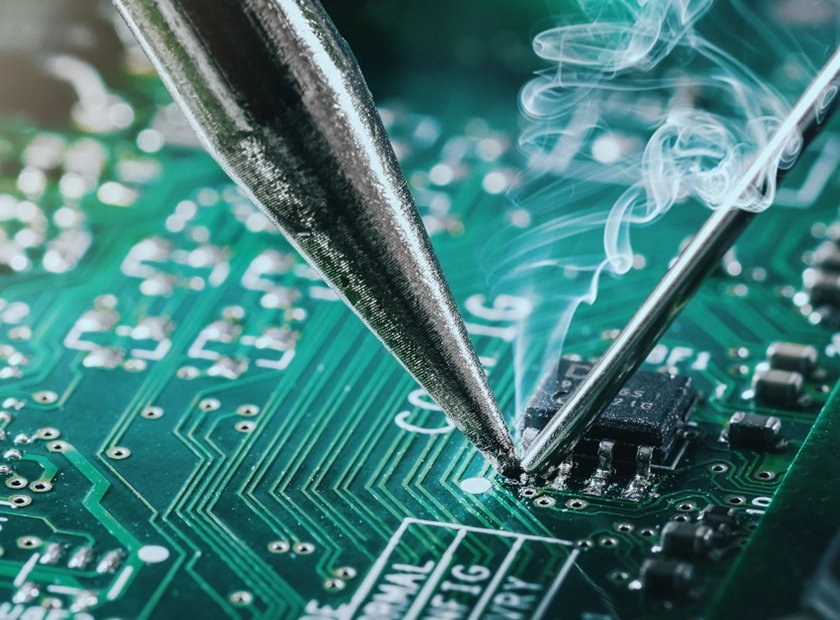
Why Solder Pad Integrity is Non-Negotiable in Modern PCB Design
May 08, 2025
In the intricate landscape of modern electronics, where miniaturization and complexity reign supreme, the humble solder pad often goes unnoticed. Yet, these precisely engineered conductive areas are the linchpins of Printed Circuit Board (PCB) functionality, serving as the critical interface between components and the board itself. Far from being mere dots of metal, the design, type, and soldering quality of these pads dictate the reliability, performance, and longevity of virtually every electronic device, from sophisticated medical implants to everyday consumer gadgets. This exploration delves into the foundational role of pad soldering, the diversity of pad designs, and the best practices essential for forging connections that last.
Bridging Worlds: The Fundamental Purpose of Solder Pads
At its core, pad soldering is the art and science of creating robust electromechanical connections. Solder pads on a PCB are meticulously designed locations where component leads or terminations are affixed using solder. This molten alloy, upon solidifying, doesn't just hold a component in place; it forms a conductive pathway essential for electrical current flow and signal integrity. A flawlessly executed solder joint ensures low resistance, consistent performance, and mechanical strength, capable of withstanding operational stresses such as vibration and thermal cycling. Conversely, a poorly designed or improperly soldered pad can be the Achilles' heel of an entire system, leading to intermittent faults, signal degradation, or outright circuit failure.

Circuit-Board-Manufacturing
A Tapestry of Pads: Tailoring Design to Application and Component Characteristics
The world of solder pads is not monolithic; its design philosophy and morphology are highly contextual. When selecting or designing pads, engineers must deeply consider the type, size, and pin configuration of the components used, as well as the operating environment and performance requirements of the final product. Each pad type possesses unique advantages and suitable scenarios, collectively forming the complex yet orderly connection network on a PCB.
Through-Hole Pads (THP) – The Robust and Reliable Classic:
As a mainstay in early circuit board designs, Through-Hole Pads are favored for their exceptional mechanical strength. Their core feature is precisely drilled holes in the PCB through which component leads pass, extending to the other side of the board or terminating within the hole. During soldering, molten solder fills the hole and envelops the lead, often forming strong solder joints on both sides of the board, much like a rivet firmly securing the component. This structure enables them to withstand significant physical stress, vibration, and thermal shock, making THPs indispensable in applications requiring high reliability and durability, such as power connectors, large electrolytic capacitors, heavy-duty relays, or frequently mated interfaces. However, their "cost" is evident: each lead requires a hole penetrating the board layers, which not only consumes valuable routing space (especially in multilayer boards where vias obstruct inner-layer routing) but also makes it difficult to significantly increase component density. Consequently, they have gradually given way to surface mount technology in modern electronics pursuing ultimate miniaturization and high integration. Their soldering process often involves wave soldering or manual soldering, which are relatively less automated and efficient.
Surface Mount Pads (SMP) / Land Patterns – The Cornerstone of High Density and Automation:
Surface Mount Pads are central to the modern PCB assembly technology revolution, designed specifically for Surface Mount Devices (SMDs). SMDs no longer require leads that pass through the board; instead, they "sit" directly on corresponding pads on the PCB surface via their flat leads, Ball Grid Arrays (BGAs), or leadless packages (LGA/QFN). The design precision of these pads, commonly referred to as "Land Patterns," decisively impacts soldering quality and product reliability. A qualified land pattern requires precise definition of the pad's length, width, shape, and relative position to the component leads. For instance, the "toe" of the pad (the extension beyond the end of the component lead) ensures sufficient space for the solder to form a good meniscus fillet, facilitating inspection and providing some stress relief. The "heel" (the pad area beneath the component body) offers primary mechanical support and a thermal path. Lateral extensions of the pad aid in good solder wetting and the formation of side fillets. Industry standards like IPC provide recommended land pattern dimensions for various SMD packages, and adherence to these standards is key to ensuring high yields. Improper sizing, such as pads that are too small, can lead to insufficient solder, poor joints, or inadequate mechanical strength. Conversely, oversized pads can increase the risk of bridging or cause components to shift or "tombstone" during reflow due to uneven surface tension. The widespread adoption of SMPs has dramatically increased component integration density, simplified automated placement and soldering processes, and helped improve high-frequency performance.
Thermal Pads and Thermal Vias – The Invisible Hand of Efficient Thermal Management:
As power densities in electronic devices continue to rise, many components—such as power transistors, voltage regulators, LED driver ICs, and high-performance processors (especially BGA-packaged chips with thermal slugs)—generate substantial heat during operation. If this heat is not effectively dissipated, component temperatures will rise sharply, leading to performance degradation, reduced lifespan, or even permanent damage. To address this, thermal pads were developed. These are typically much larger copper areas than standard signal pads, designed directly beneath the heat-generating component or in close contact with its heat sink. Their primary purpose is to provide a low thermal resistance pathway, rapidly conducting heat from the component to larger copper planes within the PCB (like ground or power planes, which can act as heat sinks) or to external heat sinks. To further enhance heat dissipation, "Thermal Vias" are often densely arranged beneath the thermal pad. These are plated through-holes that connect the surface-layer thermal pad to internal conductive copper layers or to a heat-dissipating area on the opposite side of the board, acting like numerous tiny thermal pillars that significantly increase the cross-sectional area and efficiency of heat conduction. Correctly designing the number, diameter, spacing of thermal vias, and their connection to inner copper layers is crucial for ensuring stable operation of high-power devices within permissible temperature ranges, forming an indispensable part of the overall system thermal management strategy.
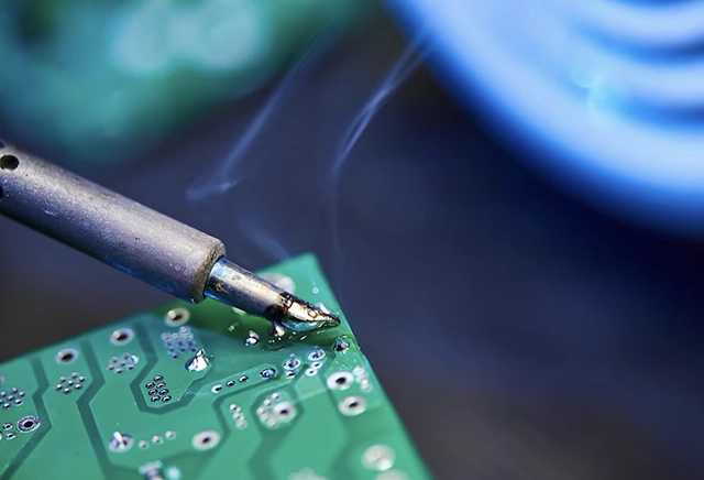
Microchip soldering
Crafting Excellence: Best Practices for Impeccable Pad Soldering
Achieving high-reliability solder joints is not a singular event but a systemic engineering effort, beginning with thoughtful consideration in the design phase and extending through every precisely controlled step of the manufacturing process. The following are key practices for ensuring superior pad soldering quality:
-
Meticulous Pad Design – Laying a Solid Foundation:
This is the foremost prerequisite for successful soldering. Strict adherence to industry standards, such as IPC-7351 (for surface mount design) and other IPC guidelines, is crucial for defining the dimensions and tolerances of land patterns. These standards are based on extensive practice and research and maximize manufacturability and reliability. During design, one must select the most appropriate pad size and shape for the specific component package type and lead dimensions. This means the pad must provide sufficient area to form a full, uniform solder fillet with a good meniscus during the reflow process. This fillet not only provides primary mechanical support and electrical connection but is also a key visual indicator of solder joint quality. Concurrently, pad design must carefully consider the spacing between adjacent pads to mitigate the risk of bridging due to excess solder or uncontrolled flow, especially in high-density layouts with fine-pitch components (like QFPs, BGAs). Furthermore, the precise definition of the Solder Mask around the pads plays a critical role. The solder mask opening is typically slightly larger than the copper pad (Non-Solder Mask Defined, NSMD) or aligned with the copper pad edge (Solder Mask Defined, SMD). A correctly designed solder mask dam effectively confines solder flow, preventing it from wicking onto non-wettable areas and helping to form consistent solder joints. Component manufacturers' datasheets should also be consulted, as they sometimes provide recommended land patterns for their specific packages.
-
Strategic Component Placement – Optimizing Overall Performance and Manufacturability:
The spatial arrangement of components on a PCB is far more than just "fitting them in." Grouping functionally related components (e.g., an IC with its corresponding decoupling capacitors, crystal oscillator, etc.) and placing them as close as possible shortens signal paths, reduces signal delay and parasitic inductance/capacitance, thereby improving signal integrity and minimizing Electromagnetic Interference (EMI) and noise. For example, by strategically placing pads, decoupling capacitors can be positioned as close as possible to the IC's power and ground pins, effectively filtering power supply noise and ensuring stable IC operation. Simultaneously, it's imperative to ensure adequate spacing between components, especially heat-generating ones. This not only facilitates air circulation and improves thermal performance, preventing localized overheating that could affect component lifespan and solder joint reliability, but also provides necessary clearance for automated placement, soldering (e.g., avoiding "shadowing effects" in wave soldering), test probe access, and potential manual rework. Rational layout can also significantly impact the uniformity and solderability of the soldering process, preventing issues like uneven heating or solder starvation in overly dense areas.
-
Controlled Solder Paste Application – Precise "Seeding" is Half the Battle:
For Surface Mount Technology (SMT), solder paste printing is the first critical process step determining solder joint quality. Solder paste is typically printed onto the PCB pads through a precisely manufactured Stencil. The stencil's thickness, as well as the size and shape of its apertures, directly determines the volume of solder paste applied to each pad. Therefore, precise control over solder paste volume and deposition location is paramount. Too little solder paste will result in insufficient solder, leading to weak joints, poor contact (cold joints), or even open circuits. Too much solder paste can easily overflow during reflow, causing short circuits between adjacent pads (solder bridges) or creating excess solder balls. The alignment accuracy of solder paste printing is also crucial; misaligned paste can cause components to shift, rotate, or even tombstone during reflow due to uneven surface tension. Modern SMT production lines are often equipped with Solder Paste Inspection (SPI) systems, which perform 3D inspection of the printed paste to ensure its volume, height, area, and position are within the permissible process window.
-
Optimized Reflow Profile – Careful "Baking" Achieves Perfect Union:
Reflow soldering is the core of the SMT process, aiming to melt the pre-printed solder paste on the pads, forming reliable electrical and mechanical connections between component leads and PCB pads. This process is achieved through a precisely controlled temperature-time curve (Reflow Profile). A typical reflow profile usually includes a preheat zone, a soak (or activation/wetting) zone, a reflow (or peak) zone, and a cooling zone. Each stage of this temperature profile must be carefully controlled and optimized:
- Preheat Zone: Gradually raises the temperature to evaporate solvents from the solder paste, activate the flux, and reduce thermal shock to components and the PCB substrate.
- Soak/Activation Zone: Allows temperatures across the PCB (with varying thermal masses) to equalize, and the flux to fully activate to remove oxides from pad and lead surfaces, preparing them for good wetting.
- Reflow/Peak Zone: Temperature rapidly rises above the solder paste's melting point, causing the paste to completely melt and wet the pads and leads, forming a liquid alloy. The peak temperature and time-above-liquidus (TAL) need precise control to ensure adequate solder flow and the formation of a good Intermetallic Compound (IMC) layer—the fundamental source of solder joint strength—while avoiding overheating or prolonged exposure that could damage sensitive components or cause PCB substrate delamination or warpage.
- Cooling Zone: Cools down at a controlled rate, allowing the molten solder to solidify and form the final solder joint structure. The cooling rate also influences the grain structure and mechanical properties of the solder joint.
Different solder paste types (e.g., leaded, lead-free), the thermal sensitivity of components, and the overall thermal mass of the PCB all necessitate corresponding adjustments and optimization of the reflow profile.
Navigating the Labyrinth: Overcoming Common Soldering Challenges
Even with stringent process controls, soldering defects can occur. Understanding the causes, manifestations, and preventive measures for these common defects is crucial for continuous improvement in design and manufacturing processes:
Solder Bridges:
- Phenomenon: An unintentional connection of excess solder between two or more adjacent pads (or leads), forming an electrical short circuit.
- Causes: Most commonly due to excessive or misaligned solder paste printing; insufficient pad-to-pad spacing (especially with fine-pitch components); improper stencil aperture design; component misplacement; or excessive solder flow/poor control during reflow.
- Impact: Directly causes circuit shorts, functional failure, and can potentially damage components.
- Prevention/Solution: Optimize pad and stencil design (e.g., using anti-bridging aperture shapes), precisely control solder paste volume and deposition, ensure component placement accuracy, and properly design solder mask dams.
Cold Solder Joints:
- Phenomenon: The solder joint surface appears dull, rough, non-shiny, sometimes granular or cracked, with poor wetting to the surrounding areas.
- Causes: Primarily due to insufficient soldering temperature or heating time, preventing the solder from fully melting and forming a good IMC layer with the pad/lead; also can be due to severe oxidation on pad or component lead surfaces, insufficient or ineffective flux activity; or too rapid cooling.
- Impact: Poor conductivity, higher resistance, weak mechanical strength, prone to cracking under vibration or temperature changes, leading to intermittent failures or eventual complete failure.
- Prevention/Solution: Optimize the reflow temperature profile, ensuring adequate peak temperature and time-above-liquidus; use sufficiently active flux; ensure clean, oxide-free surfaces to be soldered; control the cooling rate.
Tombstoning:
- Phenomenon: Typically occurs with small, two-terminal SMD components (like chip resistors, capacitors), where one end of the component is pulled up during reflow, standing vertically on the pad like a tombstone, while the other end is suspended or makes poor contact with its pad.
- Causes: Primarily due to uneven solder paste volume on the two end pads, or asymmetry in pad size/thermal mass, leading to an imbalance in surface tension of the molten solder at either end during reflow. When solder on one end melts and creates a larger pulling force first, it lifts the component. Solder paste misregistration or component misplacement can also contribute.
- Impact: Results in an open circuit at one end of the component, leading to functional failure.
- Prevention/Solution: Ensure symmetrical design of both end pads (size, shape, connected copper area); precisely control the uniformity and alignment of solder paste deposition; optimize component placement accuracy; adjust the reflow preheat stage for more uniform temperature distribution across the PCB.
Voiding:
- Phenomenon: Formation of gas bubbles or cavities of varying sizes within the solidified solder joint (sometimes also on the surface).
- Causes: Primarily due to gases generated from flux decomposition at high temperatures that fail to escape in time, or moisture absorbed by the PCB laminate/components vaporizing at high temperatures. Volatilization of solvents in the solder paste or decomposition of organic contaminants can also produce gas.
- Impact: Voids reduce the effective conductive cross-sectional area of the solder joint, increasing resistance and lowering current-carrying capacity; they decrease the joint's thermal conductivity (particularly critical for power devices or thermal pads under BGAs that rely on the solder joint for heat dissipation); voids also act as stress concentrators, reducing the joint's mechanical strength and fatigue resistance, potentially leading to crack propagation and failure over time.
- Prevention/Solution: Select low-voiding solder pastes; optimize the reflow profile, especially during preheat and soak stages to allow sufficient time for gases to escape; ensure proper baking of PCBs and components before soldering to remove moisture; improve thermal pad and via design to provide outgassing pathways.
The Broad Impact: Where Solder Pad Soldering Integrity is Paramount
From the high-stakes reliability required in automotive and medical electronics, where failure is not an option, to the mass-produced precision in consumer electronics, robust pad soldering is a universal necessity. The selection of pad types and soldering techniques must consider component specifications, the operational environment (temperature, humidity, vibration), and overall cost-effectiveness.
In conclusion, while components and complex circuit topologies often take center stage in design, the integrity of solder pads and the quality of their soldering are the true bedrock of electronic assembly. Meticulous attention to pad design, material selection, and every aspect of process control ensures that these crucial intersections perform their silent, vital role in powering our technological world.