Currency
Toggle Nav

Elecrow Blogs
-
September 02, 2016Do you miss the gyro toys we love playing when we are young? Now this toy idea have changed to large new world with plenty of great inventions like the unmanned aerial vehicles. The gyroscope shares a variety of categories and it could be divided to sensing gyroscope and indicating gyroscope from its function. The sensing gyroscope is mainly applied to the flying automatic control system for movement control of flying objects while the indicating gyroscope is mainly used in driving and pilot meter to indicate directions. Follows please enjoy two videos, you could get more different about gyroscope from the videos. Tim Peake demonstrates gyroscope - BBC News
-
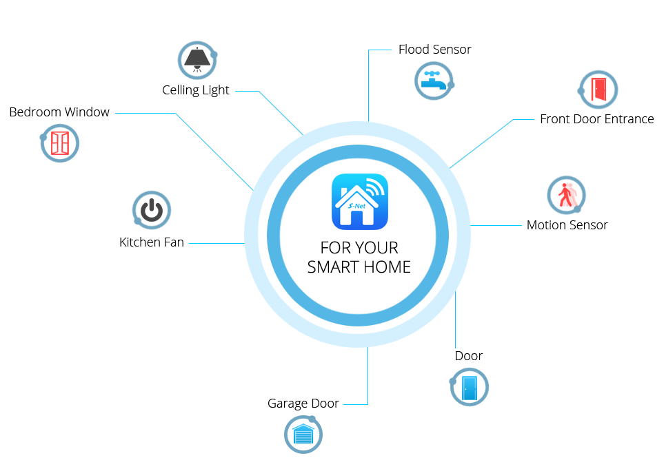
August 30, 2016The smart home must be a continuing revolution for New Age of Technology. Nowadays more and more families are pursuing the convenience of smart home for they have already been tired from hard work outside and just gonna to relax themselves and have no mood to do this and that thing when at home thus an increasing number of people are inching toward fully automated homes which is understandable and follows I will introduce several brilliant useful projects for you to turn your house into smart home.
 Hands-free
-
August 27, 2016evive is the ultimate open-source prototyping platform any maker would need. It is made for all age groups to serve a wide range of applications. Besides helping hobbyists and students in building their projects and experimental setups, it can be used by beginners to develop their making skills and by advanced users like researchers, professionals and educators to analyze and debug their projects. Six points to see its power !

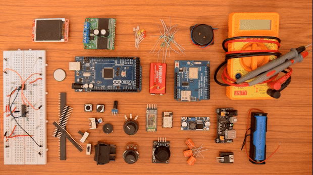 Forget dealing with humongous amount of components! When you have evive, that's all you will need. It's awesome features and innumerable components make it a one-stop solution for the maker community. And all of that at a very affordable price!

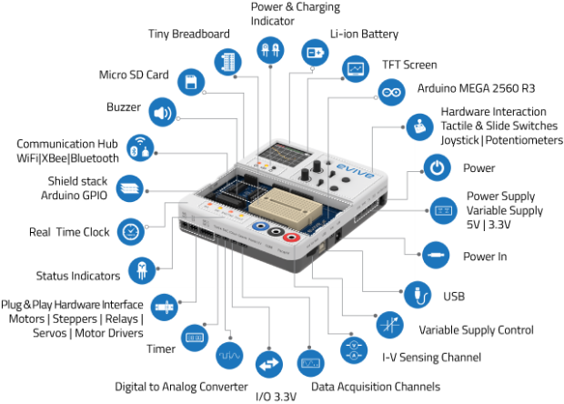 With Arduino MEGA at its heart, it offers a novel way of interacting with your hardware using it's menu based visual interface. The accurate current & voltage sensing capabilities let you collect and analyze data from your projects. The whole world of Internet of Things, with power supplies and support for sensors & actuators is available in one small portable unit. It saves your time and allows you to be more creative and innovative.

 Whether you are a high school student, a college student, a STEM tinkerer, a hobbyist, a trainer, a professional, a scientist, a professor, a researcher or anybody who loves machines coming to life, evive will expand the horizons of your creativity in a cost effective way. These modules will be provided with proper documentation to help you assemble the robots together, which can then be operated with user-friendly and intuitive on-screen menu.

 evive is an open-source hardware project. It is licensed under the Creative Commons Attribution-ShareAlike 4.0 International License. All the hardware and software related information will be made available on our GitHub repositories.
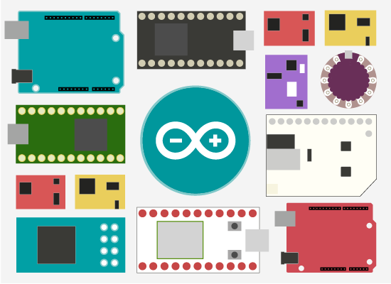
 Arduino, MATLAB SIMULINK, SCRATCH, ROS, python,Atmel Studio, eclipse, LabVIEW MakerHub etc.

-
August 25, 20163D printing is expanding quickly, with the growing popularity and uses for 3D printers every day. 3D printing can be used to prototype, create replacement parts, and is even versatile enough to print prostheses and medical implants. It will have a growing impact on our world, as more and more people gain access to these amazing machines. And a 3D printer is a manufacturing tool used to create three-dimensional artifacts that have been designed on a computer. 3D printers have a wide range of shapes, sizes, and types, but in essence they are all computer controlled additive manufacturing machines.
-
August 22, 2016
 1 A Mysterious Box- Ultrasonic Range Finder
AS a chance of new relocation of our office at that time we thought of this project to measure the distance of our furnitures and the area of the room for perfect placement of furnitures. For this project, Arduino Nano 328, is very important as our brain of rangefinder and our rangefinder's body, then you could insert Crowtail-Nano Base
1 A Mysterious Box- Ultrasonic Range Finder
AS a chance of new relocation of our office at that time we thought of this project to measure the distance of our furnitures and the area of the room for perfect placement of furnitures. For this project, Arduino Nano 328, is very important as our brain of rangefinder and our rangefinder's body, then you could insert Crowtail-Nano Base
-
August 17, 2016
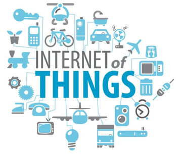 Today I wanna introduce ESP8266 NodeMCU IOT Kit for you which is an ESP8266 WiFi module with Crowtail interface for IOT Projects. IOT or internet of things is an upcoming technology that makes use of internet to control/monitor electronic/mechanical devices, automobiles and other physical devices connected to the internet. IOT gives user the ability to control more than digital things easily through a comfortable GUI over the internet. And ESP8266 NodeMCU IOT Kit is right great thing to make plenty of IOT Projects with 19 lessons tutorials and 27 kinds of Crowtail modules. Here I gonna to share several hot lessons of ESP8266 NodeMCU IOT Kit for your
-
August 15, 2016The Raspberry Pi is a series of credit card-sized single-board computers that has an ultra low cost, compared to typical computers, and it is developed in the UK by the Raspberry Pi Foundation with the intention of stimulating the teaching of basic computer science in schools to give kids a low-cost computer with which to learn how to program. The design is based on a Broadcom BCM2835 system on a chip (SoC), which includes an ARM1176JZF-S 700MHz processor, VideoCore IV GPU, and 512 megabytes of RAM. The design does not include a built-in hard disk or solid-state drive, instead relying on an SD card for booting and long-term storage. It's got a beefy quad core processor that runs at 1.2GHz, 1GB RAM, and most of the ports and capabilities that any normal computer would have. Generally, it
-
August 09, 2016Have you noticed that you're spending more time on your smartphones, tablets and other electronic devices than you are on your desktop computer? Perhaps one of the reasons is that these devices are more fun to use. With the swish of a finger, you can turn pages. By separating your forefinger and thumb, you can zoom in on text and images. You can even swirl your finger over letters to write words. With a touchscreen monitor, you can now bring this efficiency and style to your desktop computer. Touchscreen monitors have been advancing with rapid development of technology, sharing more and more functions like that of more applications support touch capabilities, which makes these monitors even more practical for a desktop setting. And adding the touchscreen capabilities to your monitor
-
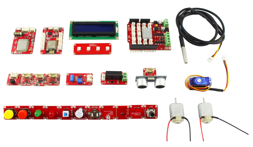
August 03, 2016As the movement of STEM is developing , we have noticed that an increasing number of people are pursuing more powerful kits for advanced new projects, so we have designed and produced the Crowtail- Deluxe Kit for arduino to satisfy all-level customers’ demands of learning and using, helping makers realize more marvelous projects. Besides, the kit involves the latest modules and the hot industry of IOT, following up recent latest technology.
 The Crowtail-
-
August 02, 2016On this 21 century, with rapid development of technology you must have heard of wireless charging and new arrival of Iphone7. They have already taken up hot place of market and people's concerns. Especially wireless charging uses electromagnetic fields to safely transfer power from a transmitting source to a receiving device for the purposes of charging or recharging a battery. And as the name suggests, it does so without the use of a physical connection which brings people much convenience and high effectivity. As for how it works ? Absolutely it works simple so you just put your hardware down and when you need it, pick it up and it’s fully charged. Wireless charging is based on the principle of magnetic resonance, or Inductive Power Transfer (IPT). This is the