Currency
Toggle Nav

Elecrow Blogs
-
November 08, 2016It has been a month since we released the "Elecrow Service Rating" survey and there are so many kind customers who participated in this questionnaire up to Nov.7th, we are sincerely appreciated to get your feedback about our service and also moved a lot to see our customers' recognition and supports to us. Here I share this survey result for all to witness Elecrow's performance and progress together and also we will present five selected loyal customers 10$ which is 1000 reward points for this participation. Congratulations !
-
November 08, 2016Acrylic laser cutting machine, also known as advertising laser engraving machine, the device is not only for acrylic processing, such as the advertising industry color version, PVC version and other generic. Elecrow provides fine acrylic laser cutting service and gets customers' recognition too.
Thanks elecrow!! always great works!! pic.twitter.com/qJqBgP8EhF
— D.F.Mac. (@tadfmac) October 27, 2016 -
November 05, 2016Temperature, humidity, and ambient pressure are key environmental parameters that can be measured at once using Bosch's fully integrated BME280 environmental sensor. This article describes how to read the environmental data from BME280 and real time data from DS1307 using Arduino and display the data on a 16×32 RGB matrix panel. [caption id="attachment_4285" align="aligncenter" width="800"]
-
November 04, 2016In my impression, makers are great group full of creativity,thoughts and action. And I also believe that every maker has an exquisite heart, showing unique love for music. So many of them have combined creation with music to make projects. Have you ever tried some? Let's see. Homemade Electronic Drum kit with Arduino Mega2560 For this project you could save much money to get an electronic drum kit at home with an Arduino mega2560 or a crowduino mega2560, first you need to prepare for these materials like wood,usb cables, EVA rubber, sensors, resistors,screws and the like. Then you could
-
November 01, 2016As we know, The Halloween Festival and The Christmas Day are of great significance in most western countries and surprisingly they also become more and more popular to most chinese people. Thus you can see unique and special chinese ways to spend these two festivals in China. First of all, the activity of pumpkin lanterns seems necessary. We like to make various grimaces of pumpkin lanterns and lighten them in the night which increase mysterious atmosphere and much fun. Certainly there are many people acting as ghosts and holding pumpkin lanterns to give away candies for children.
-
October 31, 2016This october is loaded with heavy harvest, making good farewell to shenzhen maker week and shenzhen maker faire as well as enjoying hot sales of new products in this month.So today I gonna introduce eight hot new arrivals in this month for your choice. DIY Rotating LED Display Electronic Clock Module - Blue shares display of electronic clock, date, time and temperature in turn shares brilliant functions of timing, chiming and temperature alarming and so forth enjoys over ten kinds of led display actions
-
October 27, 2016Part two, I gonna share some special and interesting products we saw on the Maker Faire. There were really hundreds of exhibitors stands showing various and funny products. Follow me and get a view below. The first stand we saw was the Intel and it really came powerfully with so large and obvious stand, there were not only VR experience zone but also drone display. Also Microsoft brought us lots of interesting products and ideas too. You can see its attracting intimating-looks free drinks auto vendor machine and IOT starter kit. Coolly kamigami brought us its unique designed robots to show the play, the robot is small but cute and operational. Surprisingly there was a large man-made electronic laser-cut flower with detection magic. When someone stands below it,
-
October 26, 20162016 Shenzhen Maker Faire has gone days ago and I was really excited to see its successful performance so these days I have been summarizing its essence and would like to share you Elecrow's view at 2016 Shenzhen Maker Faire. This Maker Faire could divide into two parts, the first is the activities it shared and the second part is various product shows of exhibitors.
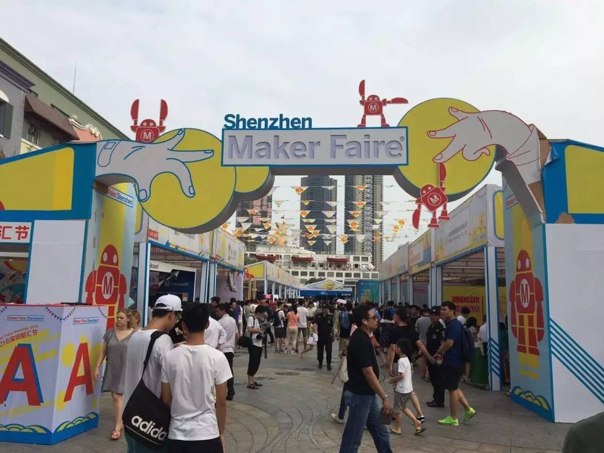 For the first part , it included abundant activities like Zao Talks,Road show, the first drone combat, 3D planetarium, Make
-
October 25, 2016LEDS are so popular among our life that you could see them almost everywhere. And this product is inexpensive but very helpful. Today I wanna introduce following projects about leds which are really fascinating and distinctive. JolliCube (8x8x8 LED Cube) With MD_Cubo Library This is a beautiful led cube ! First of all, you need to design electronic control circuit and arrange leds for your cube. Next, you can build the jigs. For the assembly part, you can build 8 layers of 8×8 led matrix and then complete the led cube with control circuit. jolliCube - 8x8x8 LED Cube Assembly Part
-
October 17, 2016
Are you a maker? Or have you had the experience of getting crazy about making or diy something interesting and useful? I think I will get "yes" for most people who loves making. Recently, I have browsed much information for any new points to write and I found five interesting and popular projects you can make at home.
How to make a Giant BristleBot using cloth washing brush
For this project, you just need these materials like 9 volt motor, 9 volt