


Story
Low-Noise Linear Power Supply for Audio (TPS7A + C-R-C Filter)
Project goal
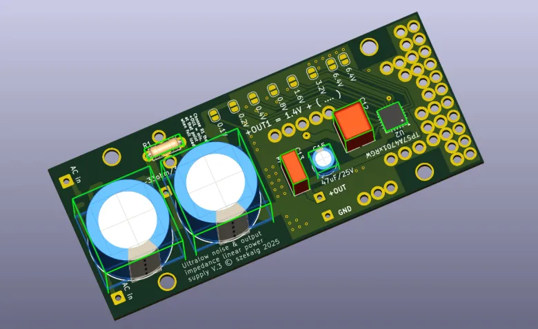
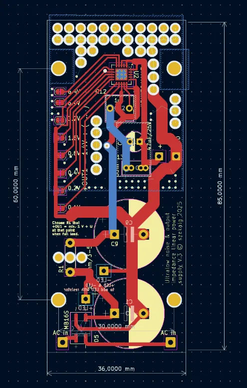
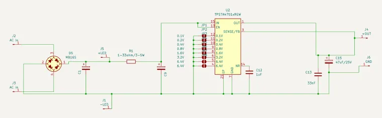
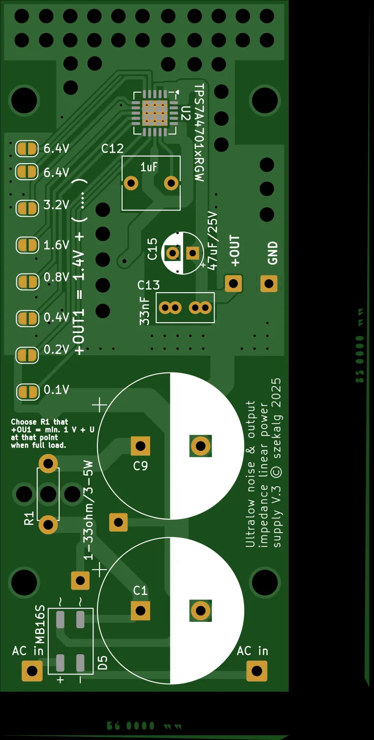
This PCB is a compact low-noise linear power supply intended for audio applications (DACs, clocks, analog output stages, I/V converters, preamps, active filters, etc.). The main goal is to obtain a very clean DC rail with low 100/120 Hz hum and reduced high-frequency “rectifier dirt” coming from the bridge.
The design combines:
- a bridge rectifier
- a reservoir capacitor C1 right after the bridge
- a C-R-C stage: C1 – R1 – C9 (where C9 is located at the LDO input)
- a precision low-noise LDO from the TPS7A family (high PSRR + low output noise)
Why C-R-C makes sense in audio
With a classic “bridge + capacitor” supply, the reservoir capacitor is charged by short, high peak currents. In audio, those pulses can translate into:
- ground noise / ground modulation
- HF spikes and EMI
- worse operating conditions for the regulator
The C-R-C filter helps because it:
1) reduces ripple before it reaches the LDO input,
2) limits charging peak currents and “calms down” the supply before the regulator,
3) reduces the risk of coupling rectifier-related noise into the “clean” section of the circuit.
LDO output noise (TI spec, indicative)
The chosen TPS7A low-noise LDO (e.g. TPS7A4701) is specified for very low output noise. According to TI, the typical output noise is roughly:
~4–5 µV RMS (10 Hz–100 kHz)
(depending on test conditions, the NR-pin capacitor and the output capacitor).
In practice: once ripple is strongly reduced by the C-R-C stage and PSRR, the limiting factor often becomes the intrinsic LDO noise and/or PCB grounding/layout details.
Estimated ripple/noise rejection (C-R-C + LDO PSRR)
The attached documents include an estimate of “total rejection” in dB for the provided variants. This is an engineering estimate calculated as:
attenuation of R1 + C9 (small-signal RC model) + LDO PSRR (summed in dB).
Important: real measured results depend on transformer regulation, bridge behavior, capacitor ESR/ESL, wiring and grounding, operating current, and voltage headroom (PSRR drops when the LDO is close to dropout).
How to select transformer + C-R-C parts (variants)
Included tables were prepared so the supply can run continuously with:
- TA = 25°C
- PCB temperature near the LDO ≤ 80°C
For each variant the tables provide:
- target Vout and maximum continuous load current
- recommended transformer VAC and minimum VA
- recommended C1 / C9 values and capacitor voltage ratings
- recommended R1, its dissipation, and suggested resistor power rating
- minimum Vin (at −10% mains) before the LDO (dropout check)
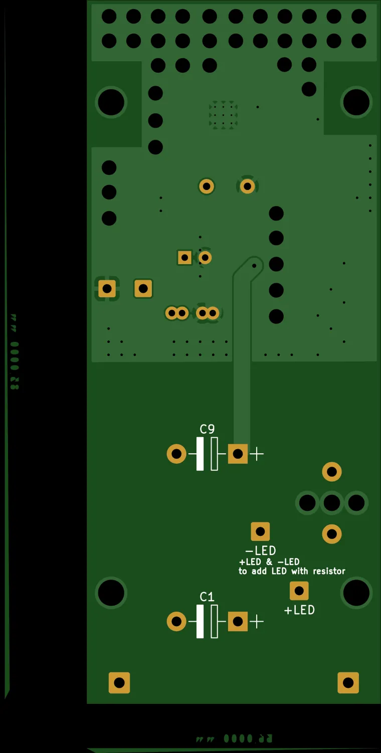
Capacitor naming (matches schematic/PCB)
- C1 = reservoir capacitor right after the bridge rectifier (“raw DC”)
- C9 = capacitor after R1, placed as close as possible to the LDO input
So the filter is: C1 – R1 – C9.
Assembly & startup (practical)
1) Power up without load and measure the DC voltage on C1 and C9 (after rectification the DC can be higher than VAC·√2).
2) Confirm that capacitors have sufficient voltage rating with margin.
3) Apply load and check:
- that the LDO is not entering dropout (output sag under load)
- temperature near the LDO and near R1 after ~10–20 minutes
4) In some variants R1 dissipates multiple watts — use a resistor with margin (e.g. 5–7 W) and provide airflow/space for heat.
Key advantages
- strong hum/ripple reduction (C-R-C + high LDO PSRR)
- low noise floor thanks to a low-noise LDO
- reduced rectifier charging pulses → less ground/EMI coupling into sensitive audio circuits
- simple, predictable linear design (easy to build and debug)
- supports multiple output voltages (3.3 V / 5 V / 12 V / 15 V) by choosing the proper variant and parts
Typical use cases
- DAC supplies (R-2R and delta-sigma)
- analog output stages and active filters
- low-jitter clock modules and sensitive digital audio sections
- voltage references and other noise-sensitive circuitry
BOM and output voltage configuration
The attached BOM is prepared for the following build:
- transformer: 9 VAC / 15 VA
- output voltage: 5.0 V
- maximum continuous load current: 0.7 A (per the tables and thermal assumptions)
For other variants (different Vout and/or transformer VAC), simply select parts using the included tables and documents (C1/C9, R1, capacitor voltage ratings, and allowable continuous load current).
Setting the output voltage (solder jumpers)
The output voltage is configured by connecting the appropriate solder jumpers on the PCB. As described in the LDO datasheet, the output follows:
Vout = 1.4 V + (sum of jumper-selected voltage increments)
In other words: 1.4 V is the base, and the final Vout is obtained by adding the increments selected with the solder jumpers.
Safety note
This board is designed to be powered from an isolated transformer secondary. Follow good safety practice when working with mains-powered equipment and always verify polarity and component voltage ratings before powering up.