


Story
Here is another reverse engineering PCB project.
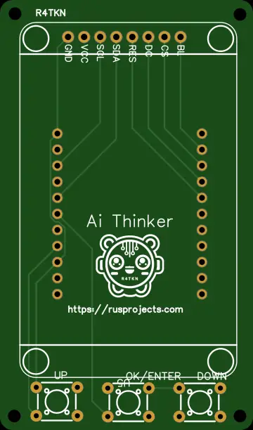
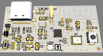
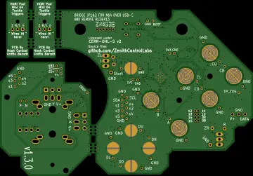
The board is two-layer , with components soldered on the TOP side and the BOT side.
The board dimensions are approximately 30 mm x 38 mm.

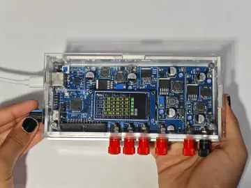
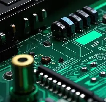
Photo of the TOP side with all components.

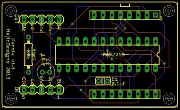
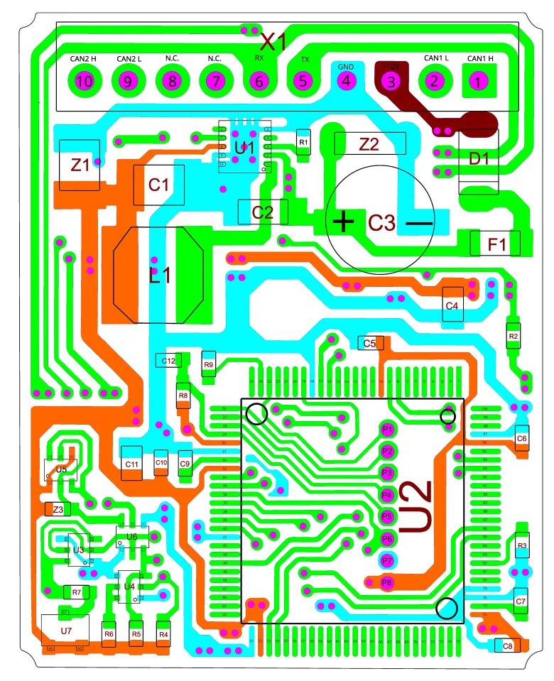
Top layer with components redrawn by me on Inkscape.

Photo of the TOP side with only some components for more legible inscriptions.

Photo of the TOP side with only some components for more legible inscriptions.

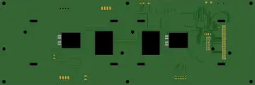
TOP layer without components and with solder mask.

TOP layer without components and withоuт solder mask

Top layer without components redrawn by me on Inkscape.

Top layer with componets and without traces redrawn by me on Inkscape.

Photo of the Bot side with all components.

Bot layer with components redrawn by me on Inkscape.

Photo of the Bot side with only some components for more legible inscriptions.
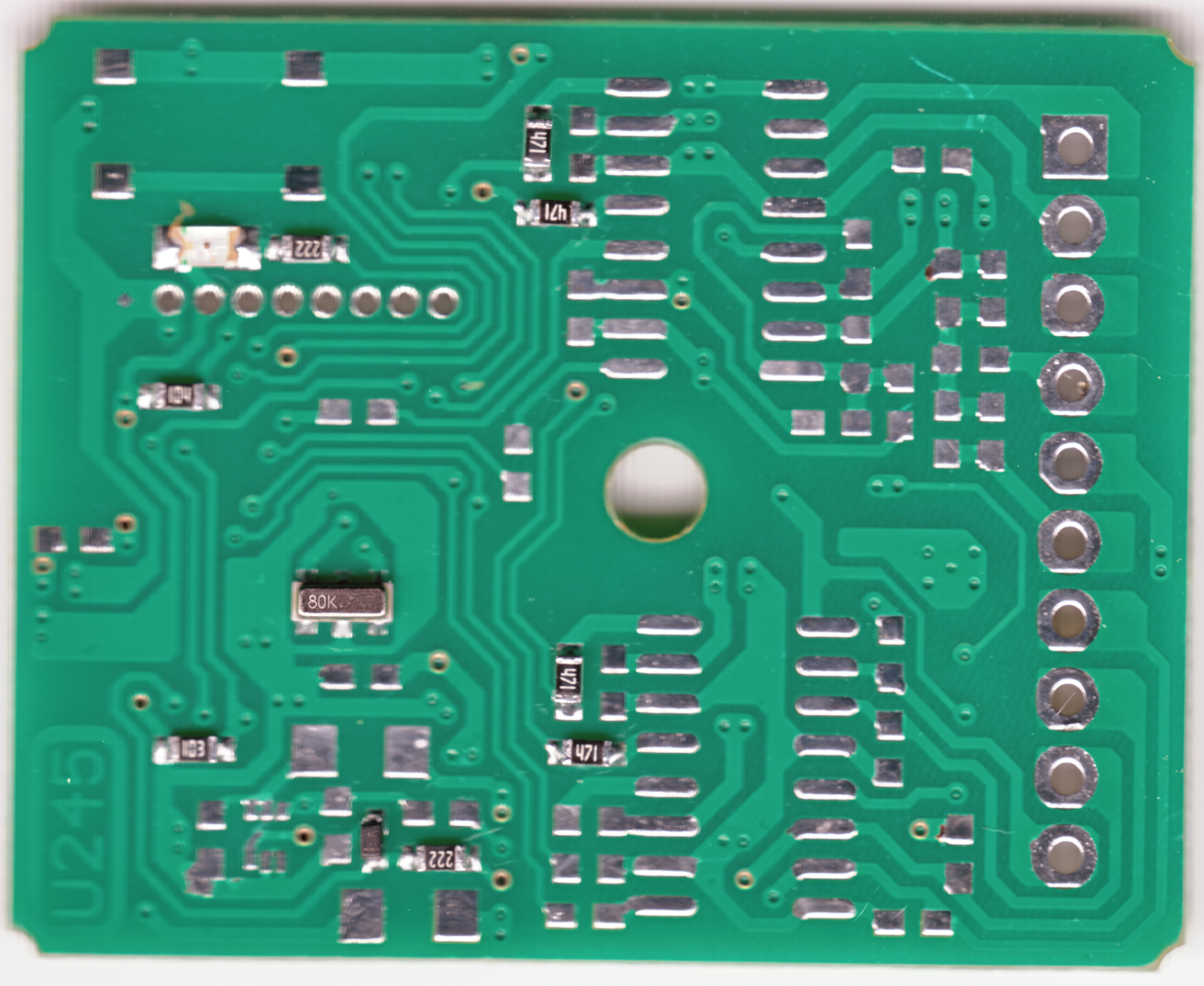
Photo of the Bot side with only some components for more legible inscriptions.

Bot layer without components and with solder mask.

Bot layer without components and withоut solder mask .

Bot layer without components redrawn by me on Inkscape.

Bot layer with components and without traces redrawn by me on Inkscape.
In the attached file you can find all layers redrawn by me on Inkscape : VIAS , TOP traces , TOP components Only , TOP paste mask ,
BOT traces , BOT components Only , BOT paste mask.