


Story
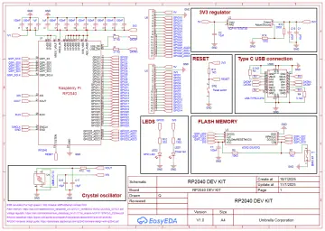
Here is another 4 layer reverse engineering PCB project.
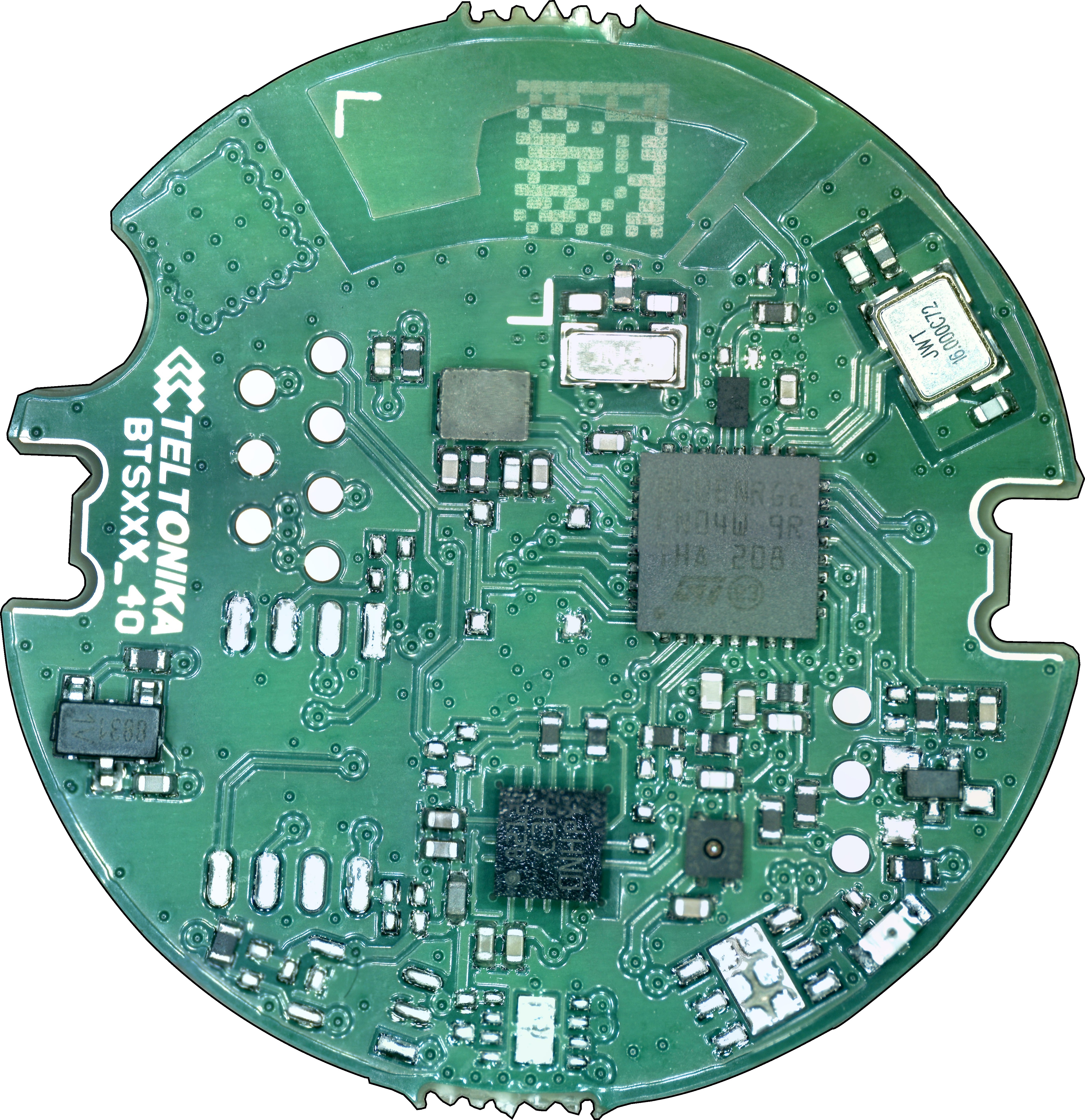
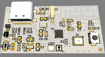
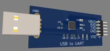
TOP with components.
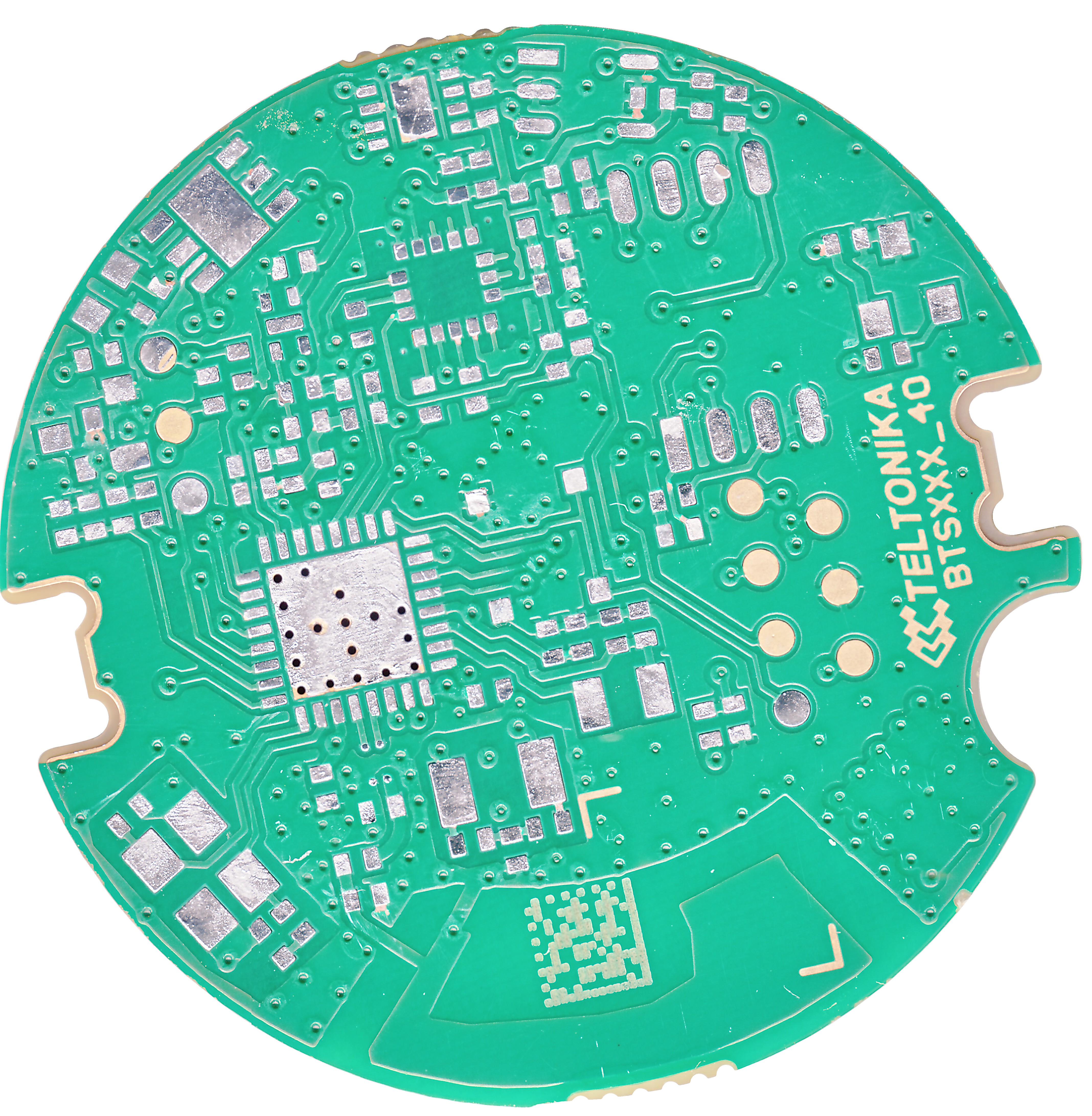
TOP without components
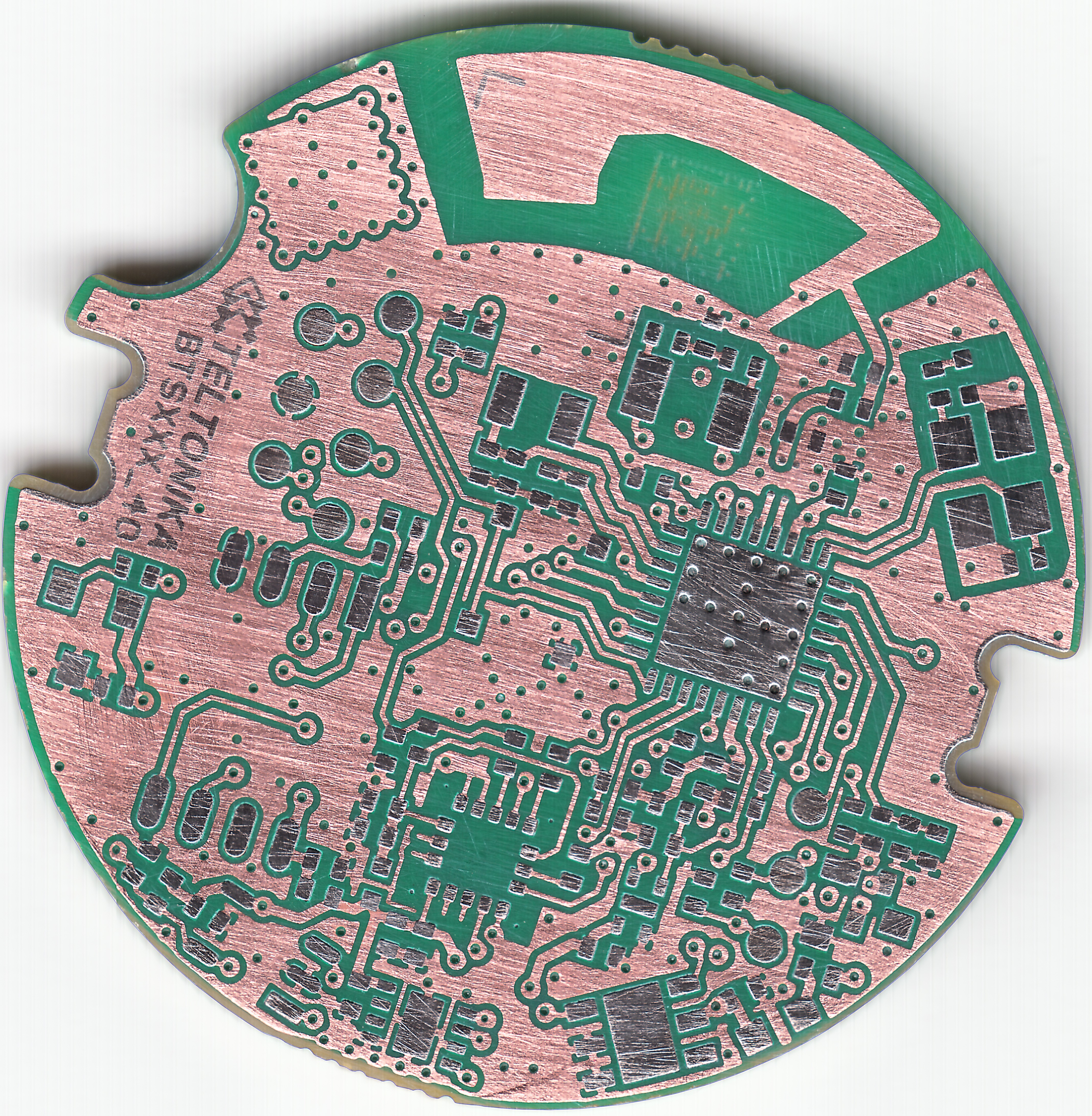
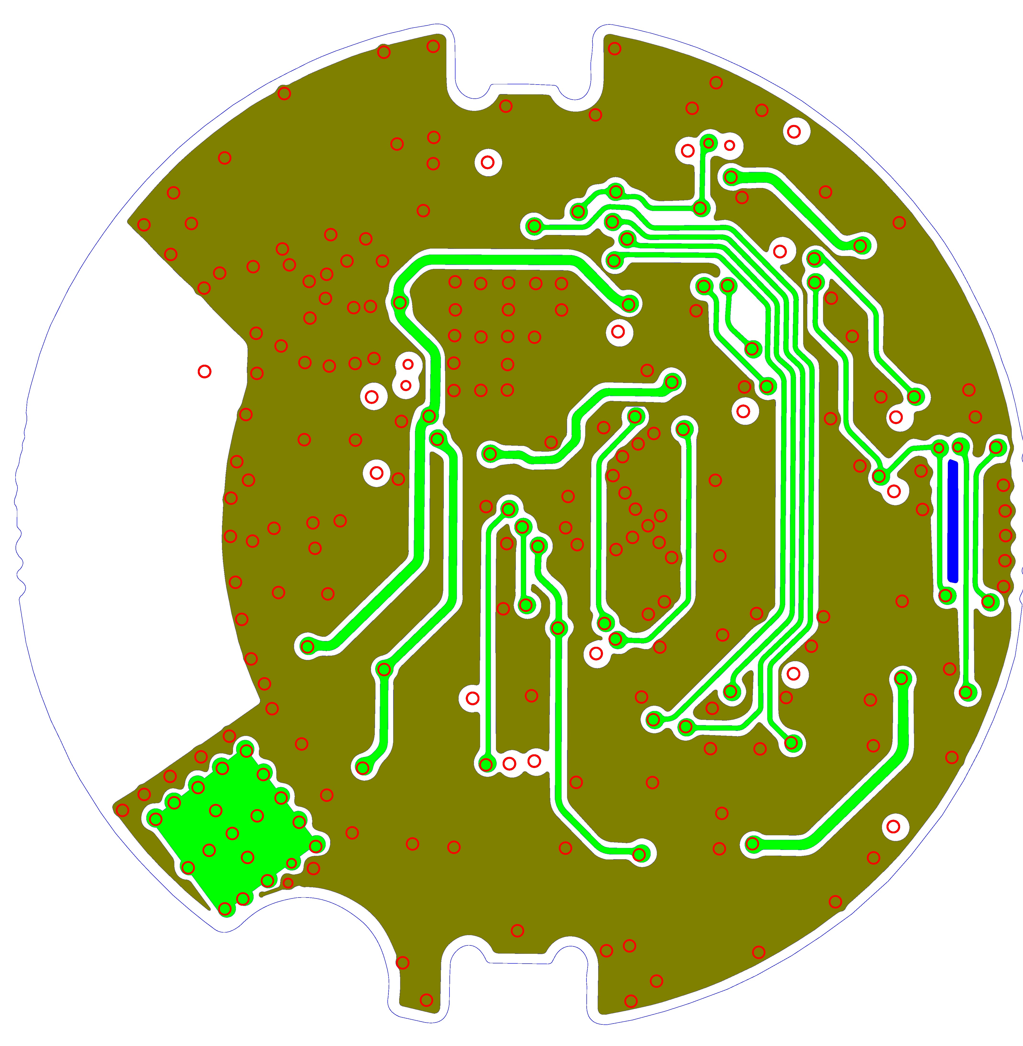
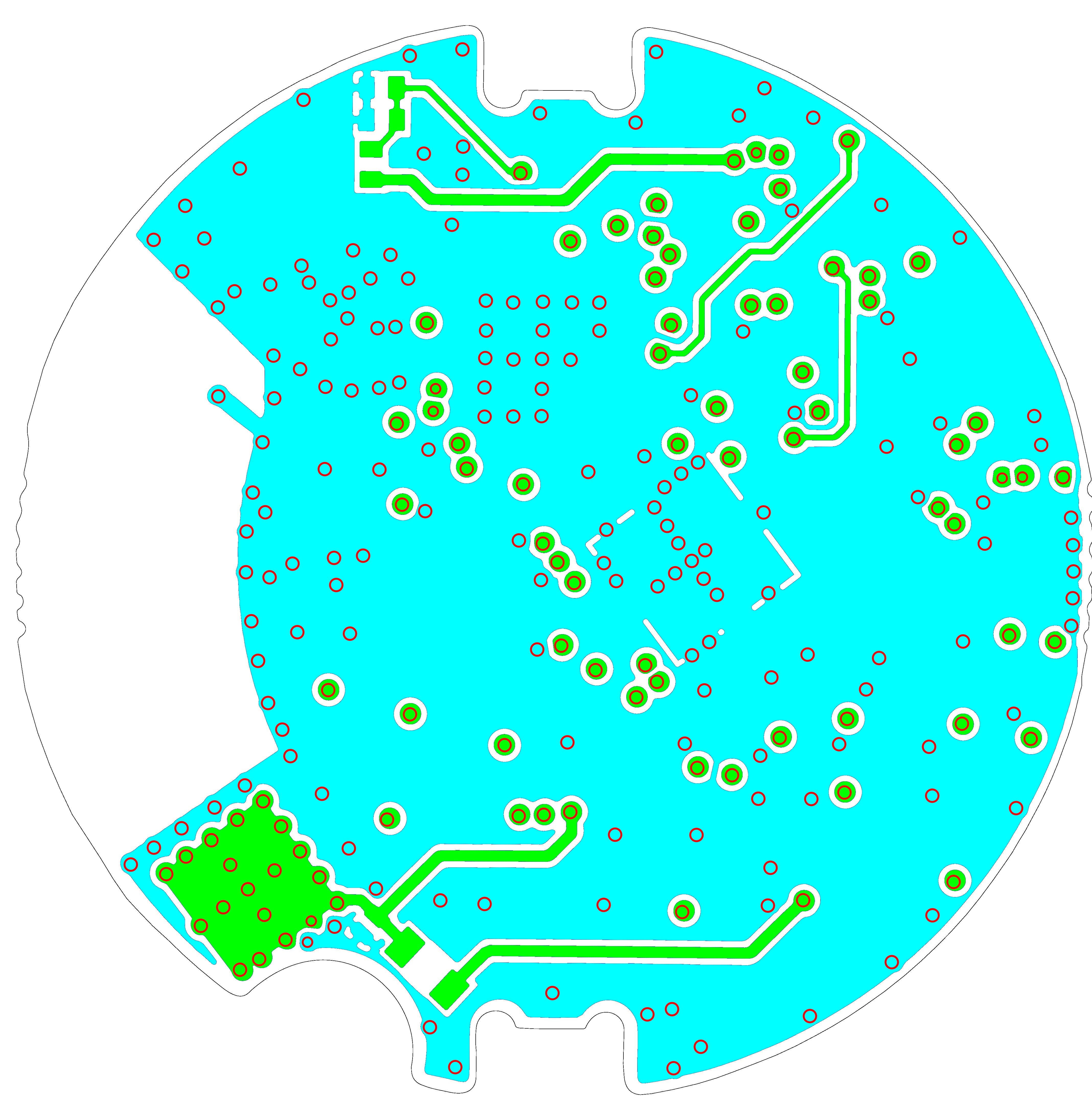
TOP without components and solder mask
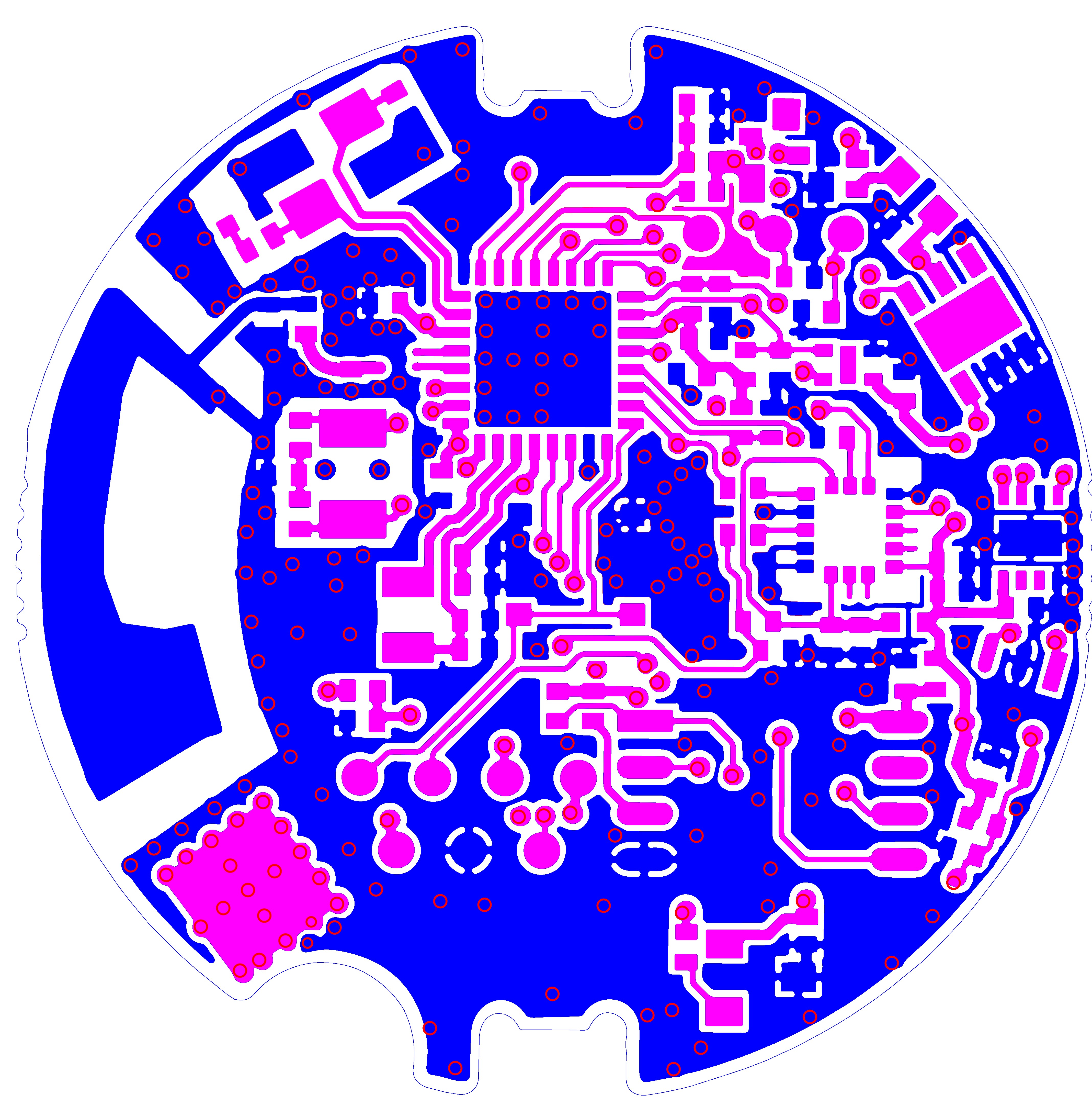
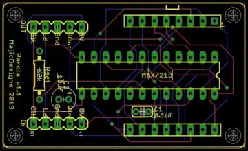
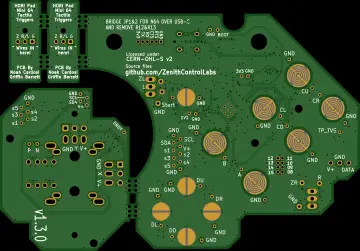
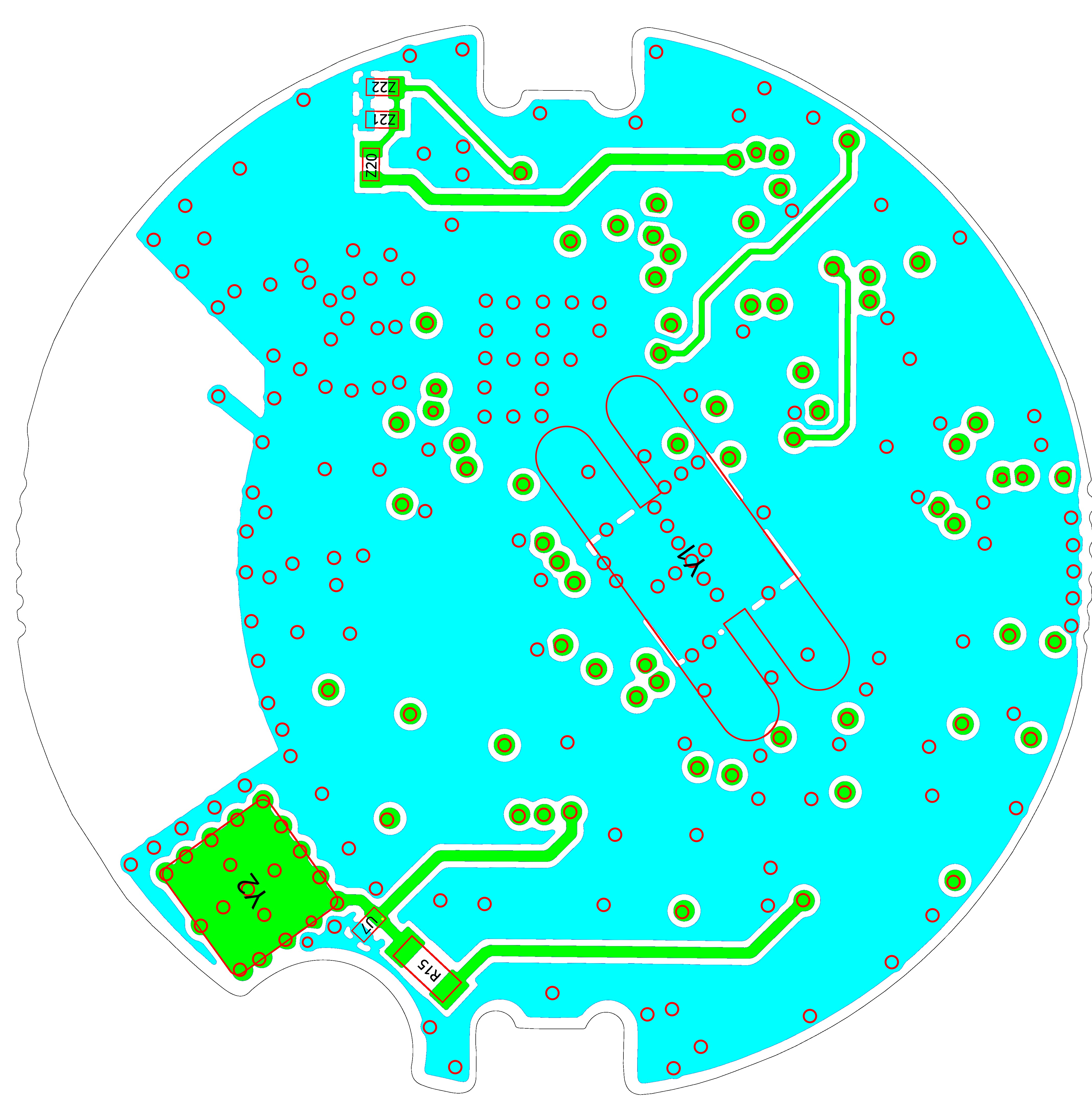
TOP from SVG drawn by me.
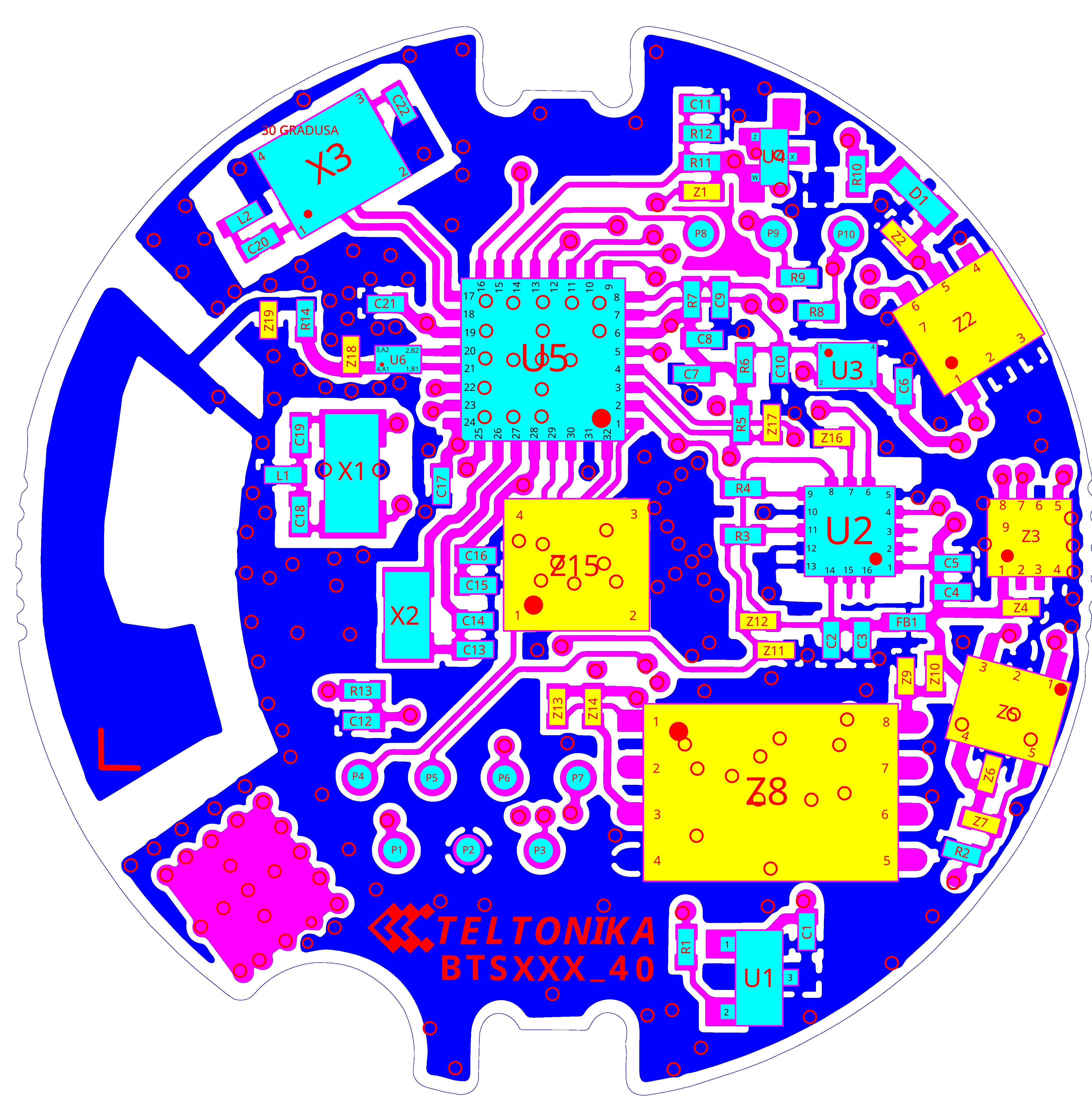
TOP with components from SVG drawn by me.
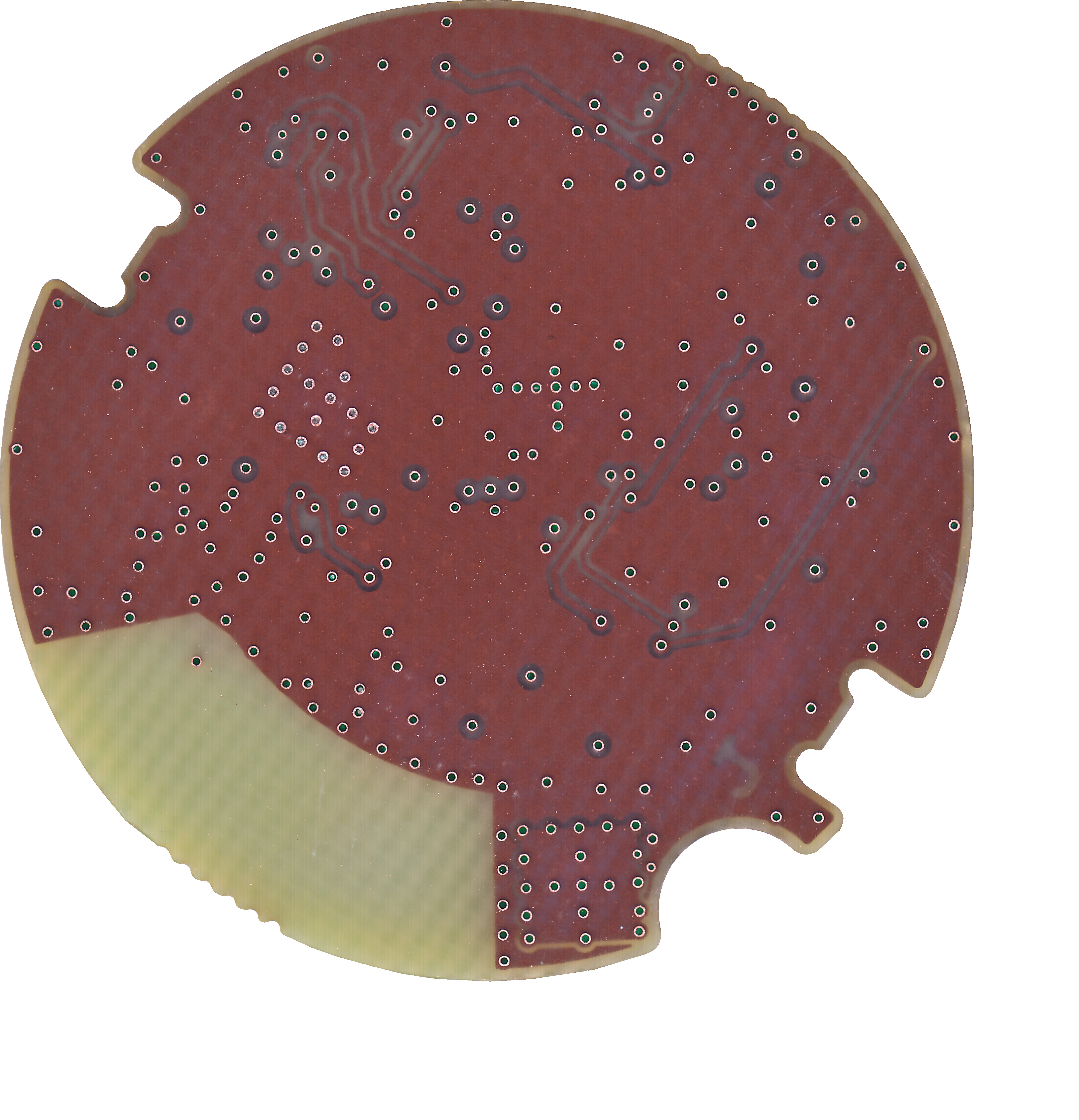
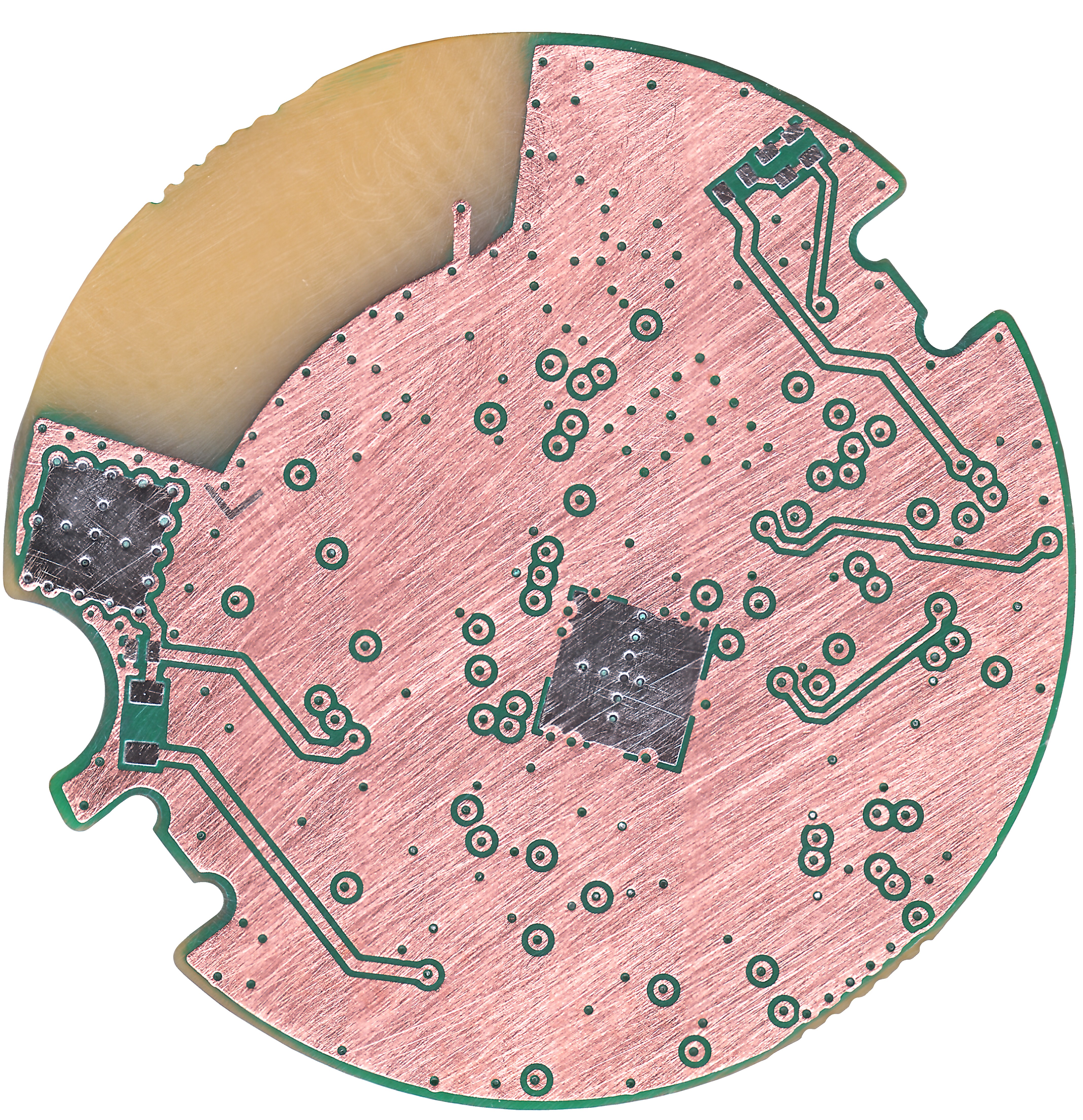
Inner layer 1 .The glass textolite between the top and inner layer 1 has not yet been completely removed.
The glass textolite between the layers is thin and becomes almost transparent.
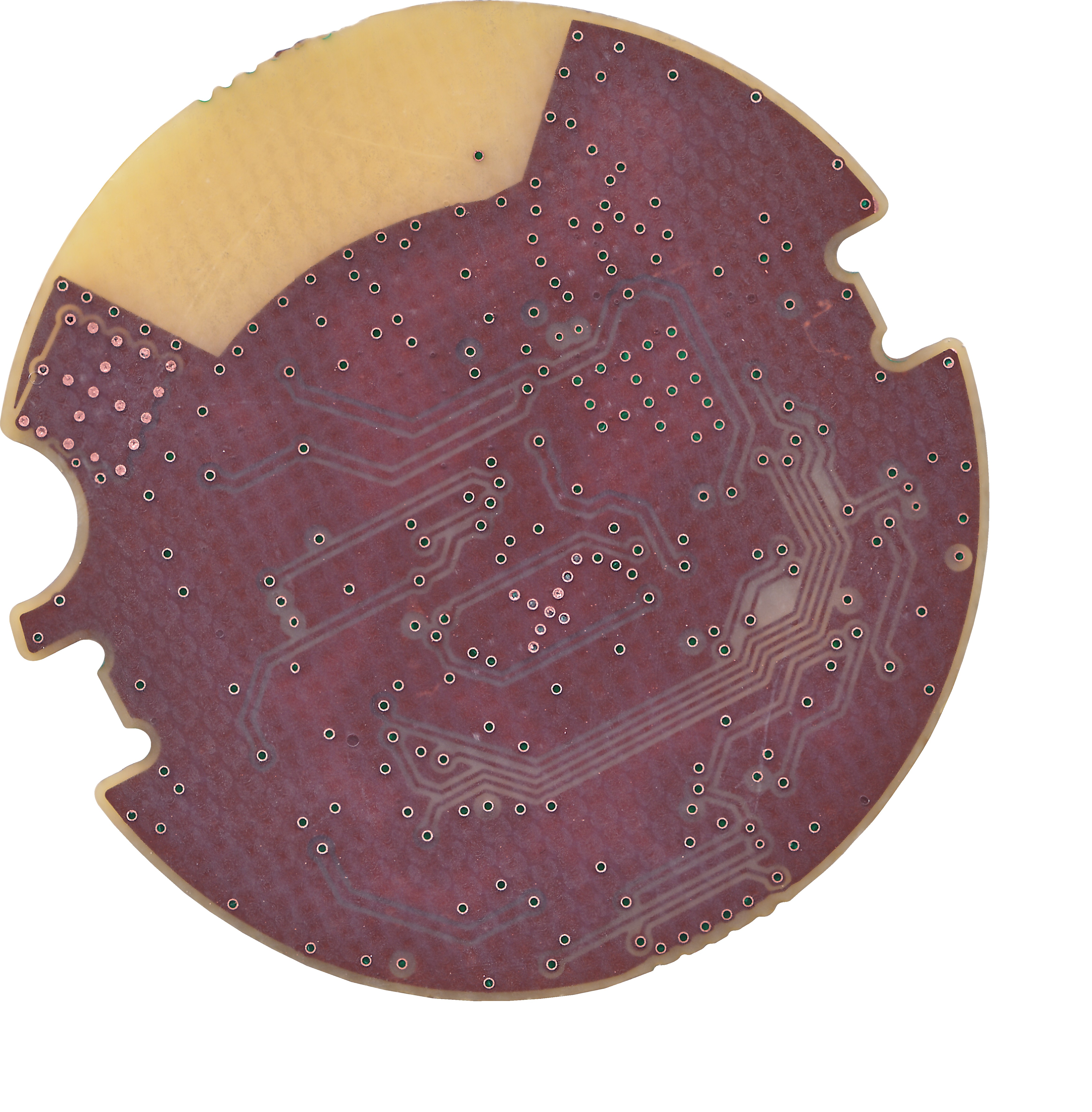
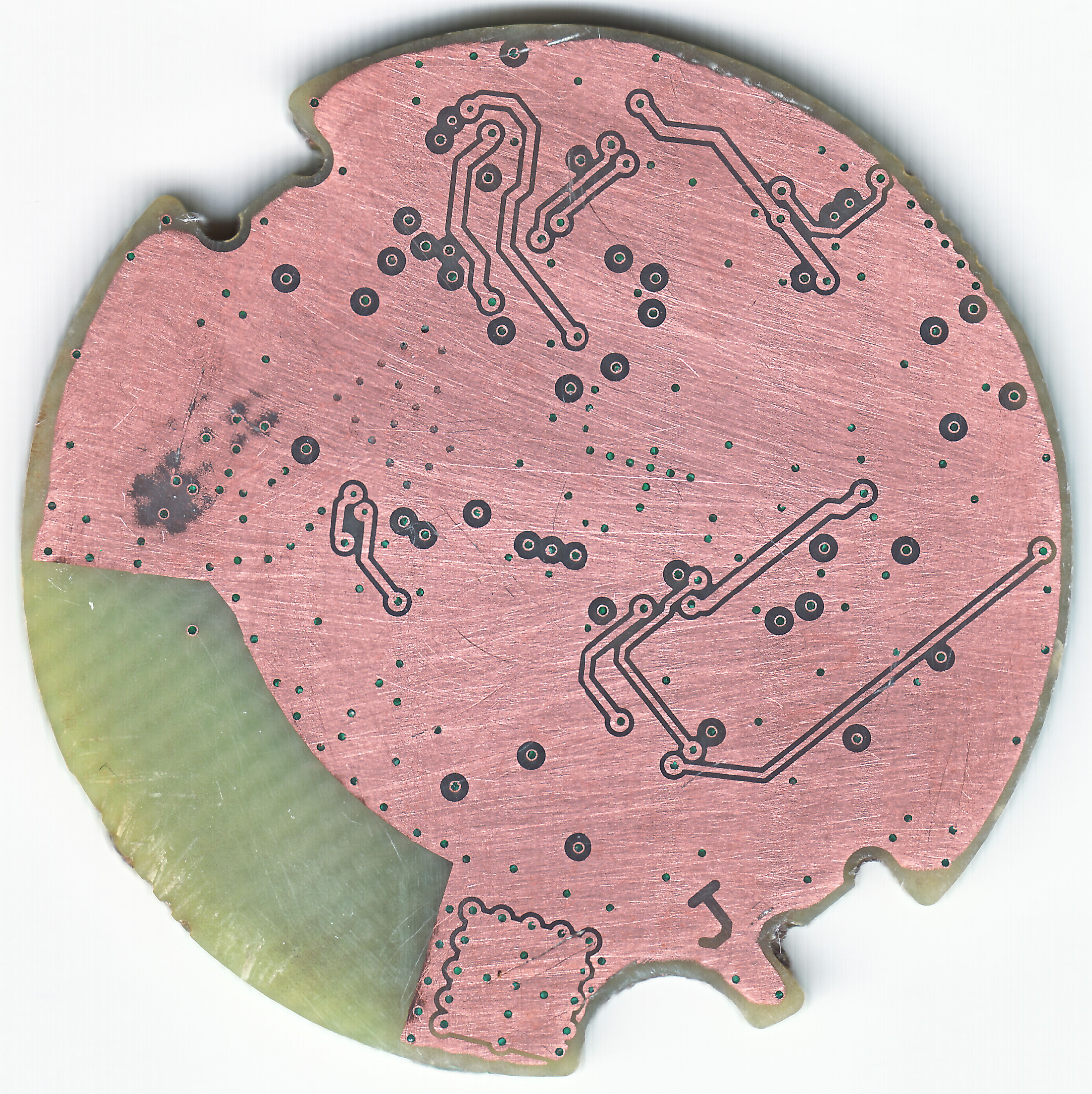
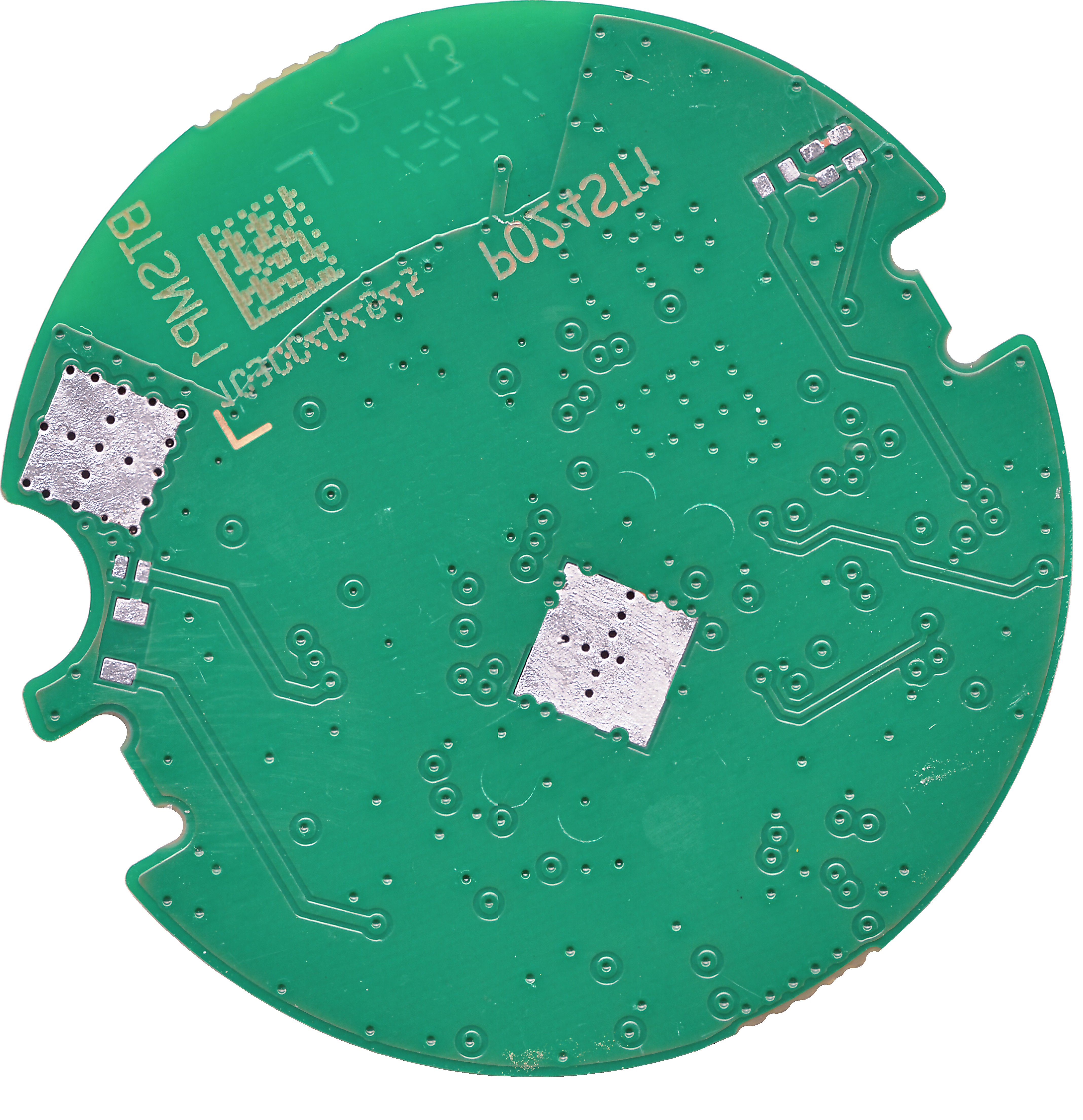
The glass textolite between the top and inner layer 1 has been completely removed.
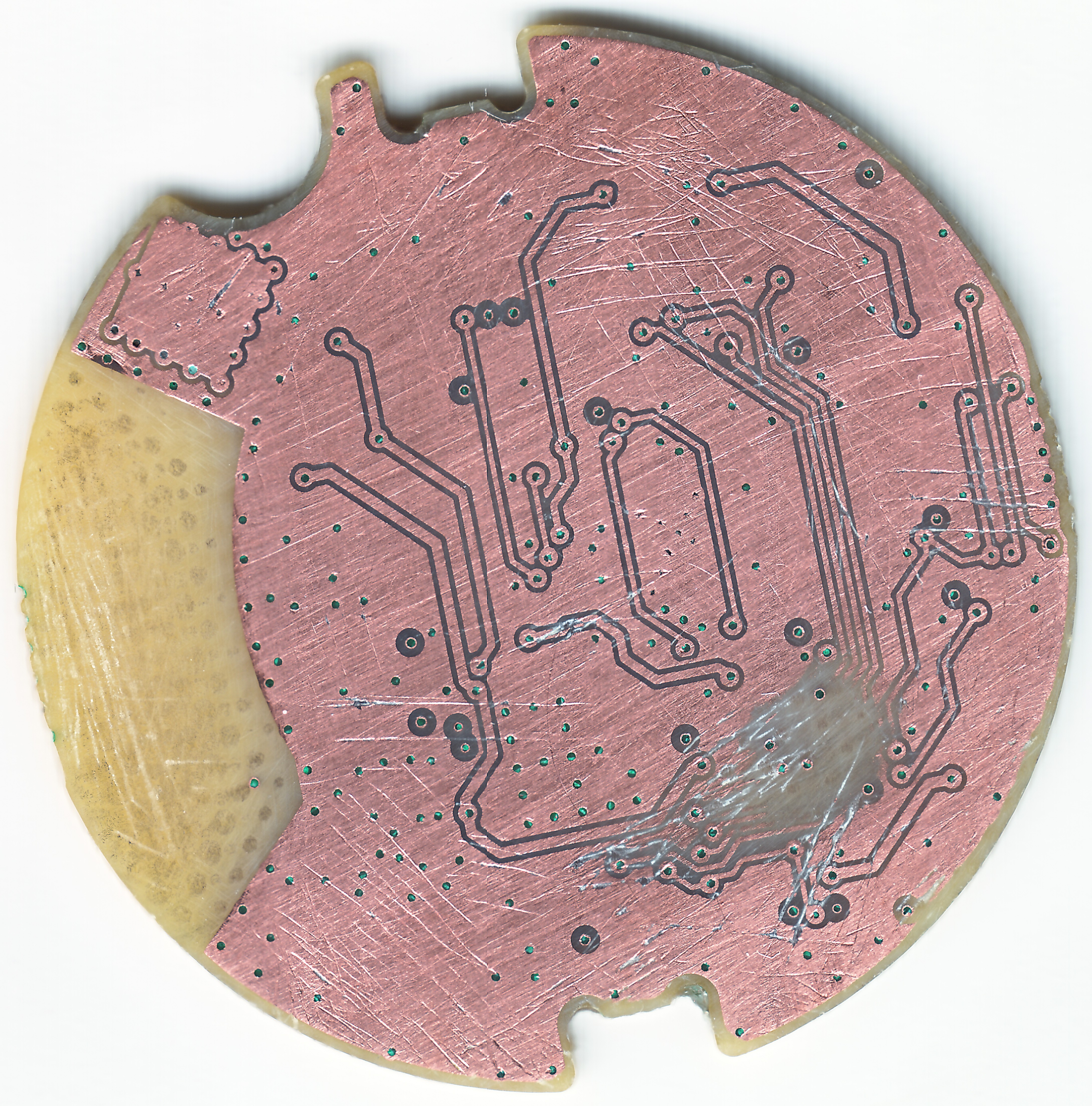
I have milled away part of the traces on Inner layer 1.
There is always such a risk - that's why you should scan slightly before reaching the inner layer.
The glass textolite between the layers is thin and becomes almost transparent.
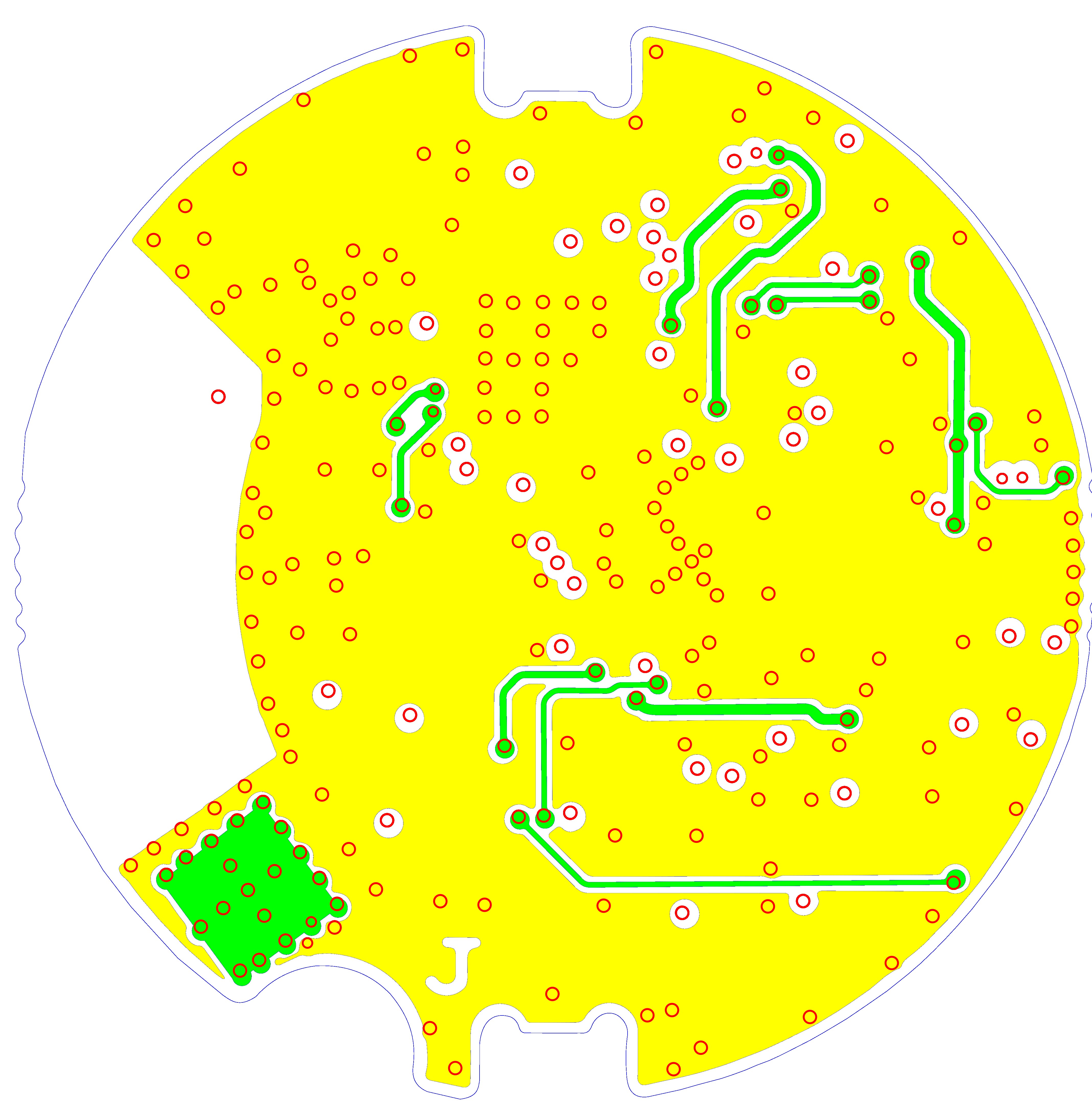
Inner layer 1 from SVG drawn by me.
Inner layer 2 .The glass textolite between the BOT and inner layer 2 has not yet been completely removed.
The glass textolite between the layers is thin and becomes almost transparent.
The glass textolite between the BOT and inner layer 2 has been completely removed.
Inner layer 2 from SVG drawn by me.
BOT from SVG drawn by me.
BOT with components from SVG drawn by me.
BOT without components and solder mask
BOT without components and with solder mask.
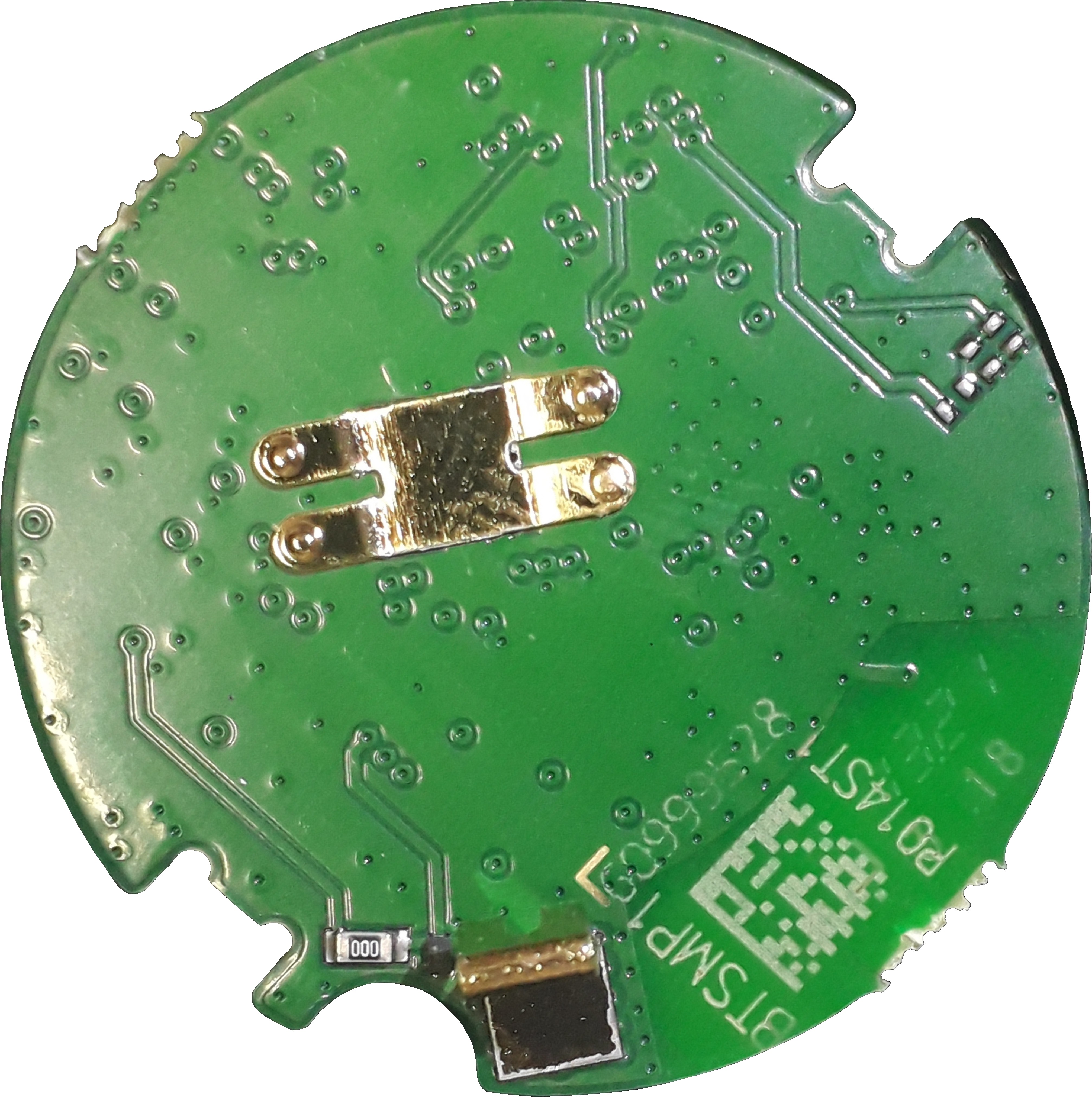
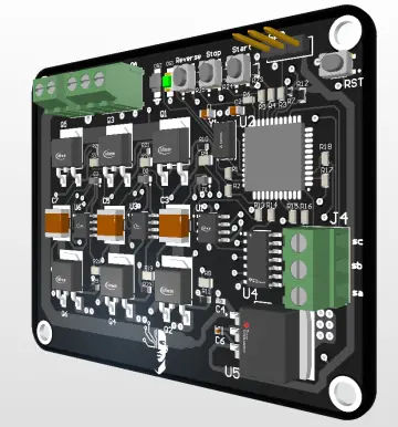
BOT with components.