


Story

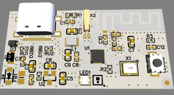
 The first thing that needs to be done is to take photos of the board as it is, with all components in place.The photos need to be clear enough so that the orientation of the components is visible—for example, where pin 1 of an IC is located.

I recommend taking separate high-resolution photos of the markings on all active components that cannot be read from the general photo. After that, on the general photo I use Inkscape to add the component names and their orientations.
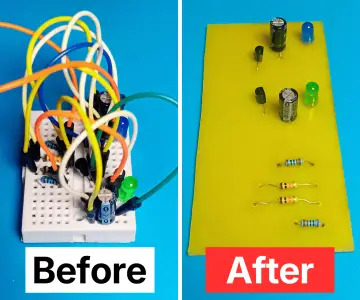
Then I desolder the components one by one. The desoldered components are soldered onto a prototyping board—capacitors in one row, resistors in another. I arrange them so they follow the numbering: first C1, next to it C2, and so on. This will make later measurements with a multimeter much more convenient.
 |
 |
 |
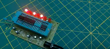
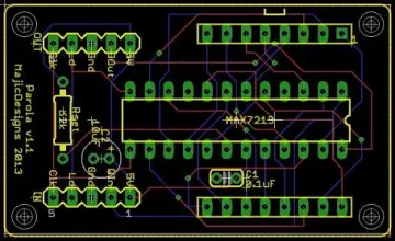
Here is an example from another project.
Once you have desoldered all components and soldered them onto the prototyping board, take a photo of the prototyping board with the components. Using Inkscape, add the component names onto the photo of the prototyping board so you know where each component is located on the experimental board.Use desoldering braid to remove the solder from the board—on both sides.After that, clean the board with solvent (e.g., paint thinner).
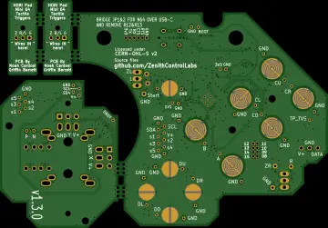
Scan both sides of the board with a scanner. For this PCB, I used an HP SCANJET SJ300 scanner at a resolution of 1200 DPI. It's not the best, but it works for this board.
Here is the HP SCANJET SJ300 scanner.
 I recommend scanning the board at several different resolutions. If the board is scanned at a very high resolution, the scanner may not be able to capture the entire board at once. In that case, scan the board in overlapping sections.To assemble a complete image of the entire board (TOP or BOT), I use Microsoft Image Composite Editor (ICE). It’s free and works very well. It can no longer be downloaded from Microsoft’s website—at least I couldn’t find it—but it is still available on the internet.Warning – very important: do not use the scanner’s image cleanup functions. If you use this feature, you may lose important details of the board. I learned this when I was reverse-engineering a 6-layer board and had this setting turned on. Some of the blind vias were so obscured that I couldn’t distinguish them.
 TOP with solder mask
 BOT with solder mask
After you have scanned the board with the solder mask (solder stop mask / solder resist), it needs to be removed.To remove the solder resist, I recommend using a glass fibre contact cleaner brush. It works slowly, but the results are very good. I use the one from Bernstein – part number: 2-166.
![]()
I have tried using sandpaper – the result is not good.In the photos of the TOP side, I used a wire brush—you can see the result—it looks messy. After you have removed the solder resist, clean the board with paint thinner/solvent and scan it again. The image of the copper may appear very dark—rotate the board by 45°, 90°, or 180° (trial and error) relative to the previous scan. This way, you can find an angle where the copper appears much shinier. I remind you again: scan the board at several resolutions, and if the board is scanned at a very high resolution, the scanner may not be able to capture the entire board at once. In that case, scan the board in overlapping sections. To assemble a complete image of the entire board (TOP or BOT), I use Microsoft Image Composite Editor (ICE).Now, several options can be used.
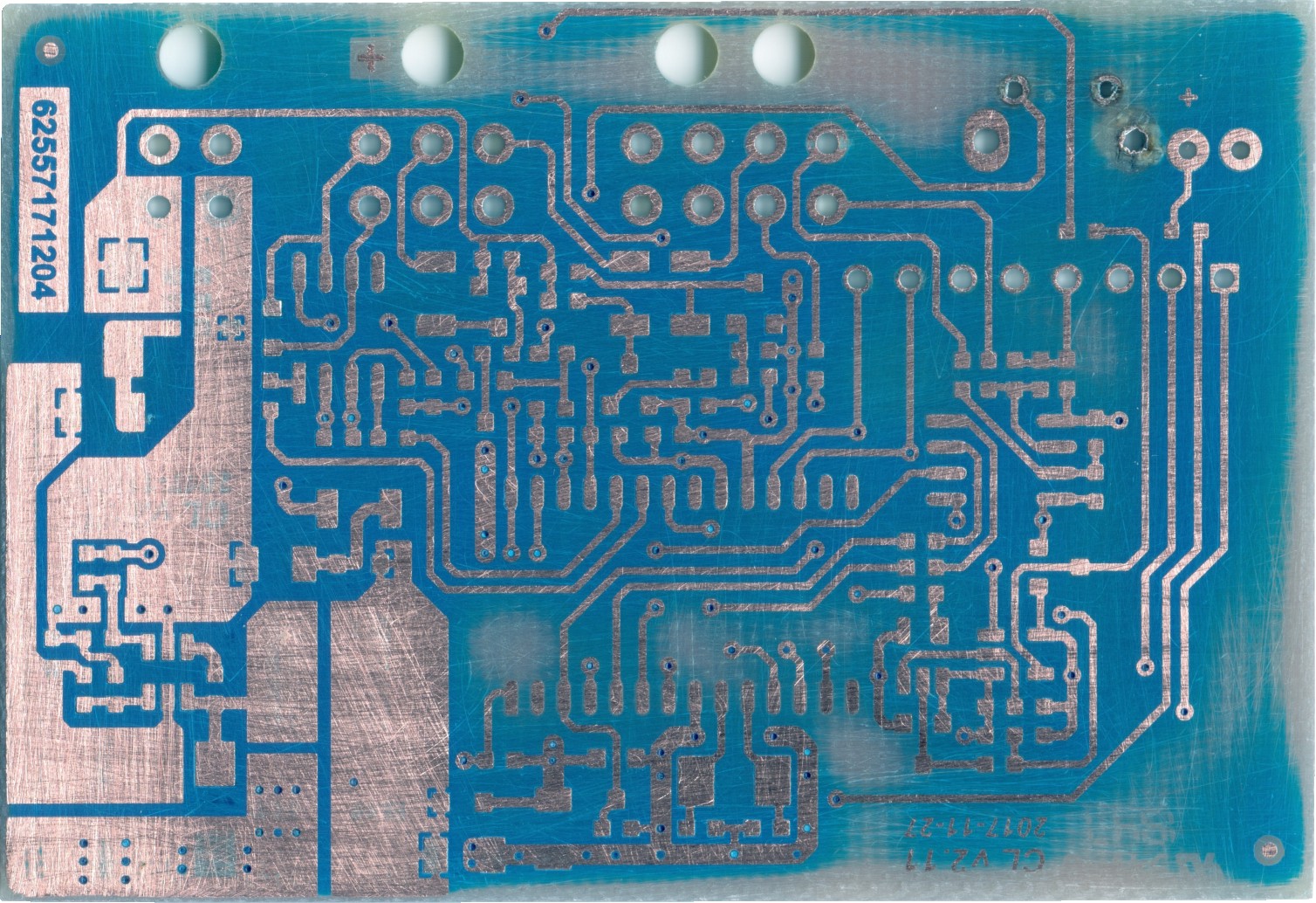 TOP without solder mask
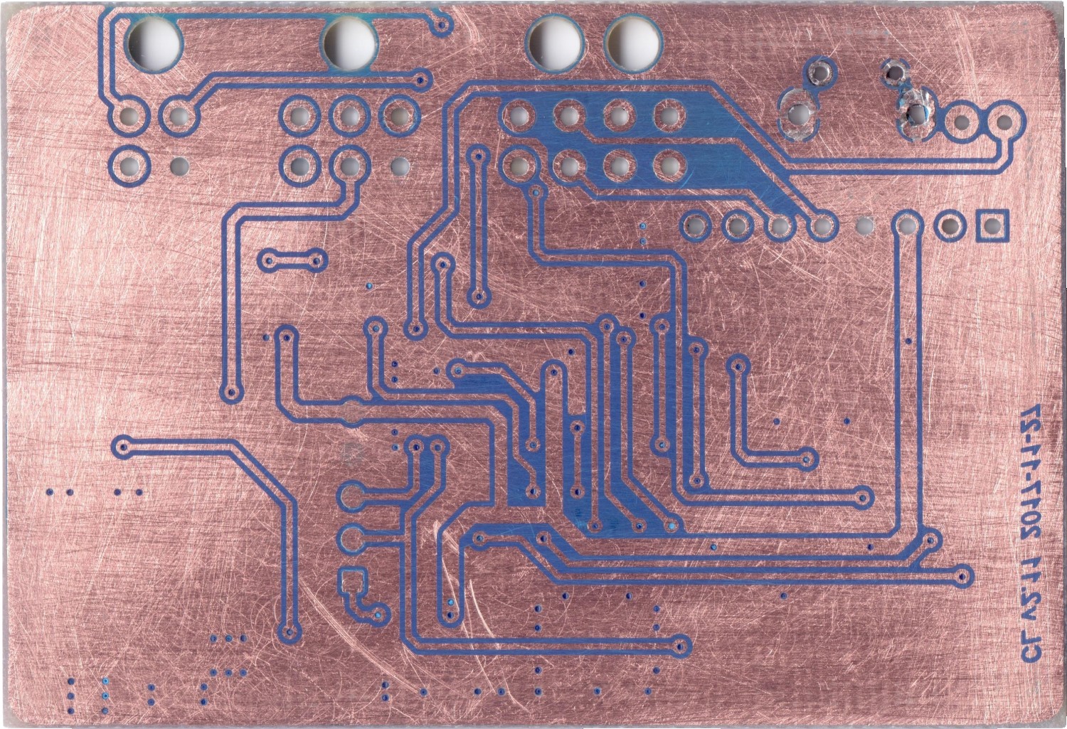
BOT without solder mask
After we have scanned TOP and BOT, we must make it so that each track, label, and via is a separate object. It can be done in several ways
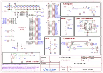
The first—the one I us is : with Inkscape, on the scanned image, I draw the traces, component names, top and bottom masks, and top and bottom paste on separate layers. It’s a lot of work, but the result is reliable. All layers that I have drawn are in a single SVG file. To open the file, extract the archive and then open it with Inkscape. Attention: I have intentionally made some layers invisible. You simply need to set them to be visible. Otherwise, it will look like an airplane crash.
Option 2: use Sprint Layout 6.0. It’s a very nice program that allows you to import images and draw over them. It has ready-made footprints. Essentially, it’s a CAD program oriented towards PCB reverse engineering. It works very well, but I encountered problems when I needed to use polygons. With Sprint Layout 6.0, you can directly export to Gerbers. The project can also be saved—if I remember correctly, this doesn’t work in the demo version.
Option 3: use Image to PCB—a program that recognizes traces and vias based on defined colors. It generates Gerbers, but as far as I remember, you still need to draw the traces and vias manually.
Option X: use a CAD system— KiCad , Altium , Zuken Cadstar , Cadence , PADS , Expedition Enterprise, and others.
Option Y: for one that I don’t know, but someone else has already used :) .