







Story
They needed it to become a product people could actually wear — thinner, lighter, and lasting a week. They also needed it fast, with a hardware team that could take the whole thing from schematic to shipped units.
This is how we approached it.
What the prototype looked like
The original build was honest engineering: an nRF52840 dev kit, a MAX30102 breakout for optical heart rate, a TMP117 for skin temperature, a 1.28" round LCD, and a 200 mAh LiPo. It worked, but the stack was 11mm thick, the BLE connection dropped whenever the display refreshed, and the optical sensor readings drifted badly during motion.
The startup had two firmware engineers but no hardware team. They were looking to hire embedded developer and a PCB designer who could own the electronics end to end. That's where we came in.
Component selection
We started by trimming the BOM. The nRF52840 stayed — it has the BLE stack, the PPI for low-power sensor scheduling, and enough RAM for their algorithms. We moved from the MAX30102 breakout to a MAX86176, which handles both PPG and ECG with better ambient light rejection. For motion, we swapped the dev board's LSM6DS3 for a BMI270, mostly for its lower power in low-ODR modes and better FIFO behavior.
The full component list on the final board:
- MCU: Nordic nRF52840 (CSP package, 48 pins)
- Optical sensor: MAX86176 PPG/ECG AFE
- IMU: Bosch BMI270
- Temperature: TI TMP117
- Display: 1.28" round AMOLED, 410x502, MIPI DSI over a small bridge
- Touch: CAP1203 capacitive controller
- PMIC: Nordic nPM1300 with integrated fuel gauge
- Charger: BQ25120A
- Haptics: DRV2605L driver with an LRA
- Memory: 4MB external flash (W25Q32) for workout logs
- Antenna: 2.4 GHz chip antenna with a matching network we tuned on the bench
- Battery: 300 mAh LiPo, custom pouch shape
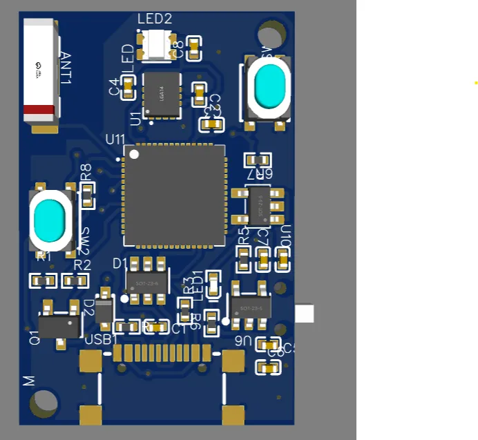
That's 11 active ICs plus passives, all on a 32mm x 38mm board that had to fit inside a 42mm watch case.
PCB design
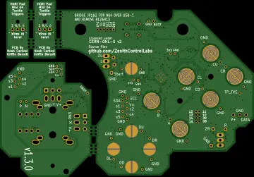
We did the layout in KiCad 8. Four layers, 0.8mm FR4, with a controlled-impedance stackup for the BLE antenna feed and the display bridge. The board is a rigid-flex design — the main PCB sits under the display, and a short flex tail wraps down to the sensor daughterboard on the wrist side. That let us put the PPG sensor directly against the skin without running long analog traces across the main board.
Some specifics that mattered:
- The MAX86176 sits on its own ground island, connected to the main ground at a single point under the AFE. PPG signals are in the nanoamp range; any ground loop shows up as noise in the heart rate trace.
- The BLE antenna keepout is 8mm on all sides, with the matching network placed within 3mm of the feed point. We tuned it with a NanoVNA and got return loss under -12 dB across the band.
- The nPM1300's inductor and the BQ25120A's input cap are placed to keep the switching loop under 5mm². That kept conducted emissions low enough to pass FCC Part 15 without a shield can.
- We used 0402 passives throughout except where 0201 was needed near the AFE. The board is dense — 187 components on 12.2 cm².
We ran three prototype spins. The first had a display bridge routing issue that caused tearing at 30 fps. The second fixed that but had a PMIC thermal issue during fast charging. The third is what shipped.
Firmware and integration
Firmware runs on Zephyr RTOS. We used the nRF Connect SDK as the base and wrote custom drivers for the MAX86176, BMI270, and the display bridge. The BLE stack uses Nordic's SoftDevice controller with a custom GATT profile — heart rate, SpO2, temperature, and a batch transfer characteristic for workout data.
Power management was the hard part. The nRF52840 spends most of its time in System ON idle, waking on a 25ms timer to sample the IMU and every 100ms to sample the AFE. The display refreshes at 30 fps only when the wrist is raised; otherwise it drops to 1 fps. We used the PPI to chain the RTC to the SPI peripheral so the CPU stays asleep during sensor reads.
Measured battery life on the final build: 6.5 days with normal use (heart rate on, notifications, 30 minutes of workout tracking per day). That's with the 300 mAh cell. The original prototype did 14 hours on 200 mAh.
What we shipped
We delivered:
- Full schematic and 4-layer rigid-flex PCB, designed in KiCad
- 3D-printed enclosure prototypes for fit checks (we do 3D design in-house)
- Zephyr firmware with OTA update support
- Production test jig and firmware for factory flashing
- 50 pre-production units assembled and validated
The startup's firmware team took over the codebase after we handed off. We stayed on for two months of integration support while they brought up their mobile app against the new GATT profile.
What we'd do differently
The display bridge was the wrong call. We picked a MIPI DSI bridge to save pins, but it added cost and a firmware headache. A parallel RGB interface would have been simpler and cheaper for a 410x502 panel. If we did this again, we'd push back on the display choice earlier.
We'd also start the antenna tuning sooner. We didn't get the VNA on the first spin until week 6, and the matching network changed twice after that. That's a week of schedule we could have recovered.
If you're building something similar
Most hardware startups hit the same wall: the prototype works, but nobody on the team has taken a board through DFM, EMC, and production test. That's the gap we fill. If you're looking to hire an embedded developer or a hardware team that can own the whole stack — schematic, layout, firmware, enclosure, and the factory — we've done it before. The smartwatch above is one of about 40 products we've taken from prototype to production.
If you want to talk through your project, the contact form on our site goes straight to our engineers, not a sales team.