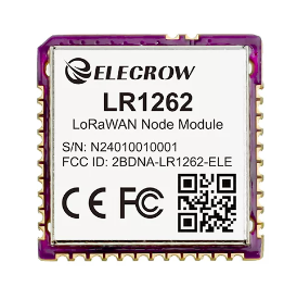
LR1262 LoRaWAN Node Module
Description
The LR1262 is a low power long range transceiver module based on the STM32WLE5CCU6 chip. It provides an easy-to-use, small size and low power solution for long range wireless data applications. The module is compliant with the LoRaWAN 1.0.3 specification for Class A, B and C standards. It can easily connect to different LoRaWAN server platforms such as TheThingsNetwork (TTN), Chirpstack, Actility and others. It also supports LoRa peer-to-peer (P2P) communication mode, which helps you quickly implement your own customised long-range LoRa network. You can configure the module's mode and operation using AT commands via the UART interface.The LR1262 also features low power consumption, making it ideal for battery-powered applications.
The LR1262 is a high-power remote module with a convenient stamp-hole form factor for easy integration into device motherboards without additional components. It supports multiple frequency plans such as EU868/US915/AU915/AS923/KR920/IN865 and is compatible with LoRaWAN® Class A/B/C protocol. In addition, the module is FCC/CE certified, making it cost-effective to quickly get your entire device certified and approved by any regulatory agency. With the built-in AT command firmware, beginners can easily create prototypes or applications with just a few simple commands. On the other hand, experienced developers can use the SDK to develop custom products.
Model: CRT01268N
Feature
- Based on STM32WLE5CCU6
- Compliant with LoRaWAN 1.0.3 specification
- Supported bands IN865, EU868, AU915, US915, KR920, RU864 and AS923-½/¾
- LoRaWAN activation via OTAA/ABP
- LoRa peer-to-peer (P2P) communication
- Developed for Keil
- Easy-to-use AT command set via UART interface
- Long range - more than 2 km with optimised antennas
- ARM Cortex-M4 32-bit
- Flash 256 kbytes with ECC
- RAM 64 kbytes
- Ultra-low power consumption of 2.2 μA in sleep mode
- Supply voltage: 2.0 V ~ 3.6 V
- Temperature range: -20°C ~ 85°C
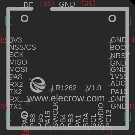
Pin Function
| Pin number | Pin name | Pin type | Alternate funtions | Additional funtions |
|---|---|---|---|---|
| 1 | GND | GND | ||
| 2 | BOOT | I/O | CM4_EVENTOUT | |
| 3 | NRST | I/O | ||
| 4 | GND | GND | ||
| 5 | GND | GND | ||
| 6 | 1V55 | |||
| 7 | ADC(PB2) | I/O | LPTIM1_OUT,I2C3_SMBA,SPI1_NSS,DEBUG_RF_SMPSRDY | COMP1_INP,COMP2_INM,ADC_IN4 |
| 8 | PA10 | I/O | RTC_REFIN,TIM1_CH3,I2C1_SDA,SPI2_MOSI/I2S2_SD,USART1_RX,DEBUG_RF_HSE32RDY,TIM17_BKIN,SM4_EVENTOUT | COMP1_INM,COMP2_INM,DAC_OUT1,ADC_IN6 |
| 9 | GND | |||
| 10 | GND | |||
| 11 | PC13 | I/O | CM4_EVENTOUT | TAMP_IN1/RTC_OUT1/RTC_TS/WKUP2 |
| 12 | SWDIO(PA13) | I/O | JTMS-SWDIO,I2C2_SMBA | ADC_IN9 |
| 13 | SCL(PA12) | I/O | TIM1_ETR,LPTIM3_IN1,I2C2_SCL,SPI1_MOSI,RF_BUSY,USART1_RTS,CM4_EVENTOUT | ADC_IN8 |
| 14 | SDA(PA11) | I/O | TIM1_CH4,TIM1_BKIN2,LPTIM3_ETR,I2C2_SDA,SPI1_MISO,USART1_CTS,DEBUG_RF_NRESET | COMP1_INM,COMP2_INM,ADC_IN7 |
| 15 | PA1 | I/O | TIM2_CH2,LPTI3_OUT,I2C1_SMBA,SPI1_SCK,USART2_RTS,LPUART1_RTS,DEBUG_PWR_REGLP2S,CM4_EVENTOUT | |
| 16 | PB3 | I/O | JTD0/TRACESWO,TIM2_CH2,SPI1_SCK,RF_IRQO,USART1_RTS,DEBUG_RF_DTB1,CM4_EVENTOUT | COMP1_INM,COMP2_INM,ADC_IN2,TAMP_IN3/WKUP3 |
| 17 | PB4 | I/O | NJTRST,I2C3_SDA,SPI1_MISO,USART1_CTS,DEBUG_RF_LDORDY,TIM17_BKIN | COMP1_INP,COMP2_INP,ADC_IN3 |
| 18 | SWCLK(PA14) | I/O | JTCK-SWCLK,LPTIM1_OUT,I2C1_SMBA,CM4_EVENTOUT | ADC_IN10 |
| 19 | PA15 | I/O | ||
| 20 | PB5 | I/O | LPTIM1_IN1,I2C1_SMBA,SPI1_MOSI,RF_IRQ1,USART1_CK,COMP2_OUT,TIM16_BKIN | |
| 21 | PB8 | I/O | TIM1_CH2N,I2C1_SCL,RF_IRQ2,TIM16_CH1,CM4_EVENTOUT | |
| 22 | PA0 | I/O | TIM2_CH1,I2C3_SMBA,I2S_CKIN,USART2_CTS,COMP1_OUT,DEBUG_PWR_REGLP1S,TIM2_ETR | TAMP_IN2/WKUP1 |
| 23 | TX1(PA2) | I/O | LSCO,TIM2_CH3,USART2_TX,LPUART1_TX,COMP2_OUT,DEBUG_PWR_LDORDY | LSCO |
| 24 | RX1(PA3) | I/O | TIM2_CH4,I2S2_MCK,USART_RX,LPUART1_RX,CM4_EVENTOUT | |
| 25 | TX2(PB6) | I/O | LPTIM1_ETR,I2C1_SCL,USART1_TX,TIM16_CH1N | |
| 26 | RX2(PB7) | I/O | LPTIM1_IN2,TIM1_BKIN,I2C1_SDA,USART1_RX,TIM17_CH1N | |
| 27 | PA8 | I/O | MCO,TIM1_CH1,SPI2_SCK/I2S2_CK,USART1_CK,LPTIM2_OUT | |
| 28 | MOSI(PA7) | I/O | TIM1_CH1N,I2C3_SCL,SPI1_MOSI,COMP2_OUT,DEBUG_SUBGHZSPI_MOSIOUT,TIM17_CH1,CM4_EVENTOUT | |
| 29 | MISO(PA6) | I/O | TIM1_BKIN.I2C2_SMBA,SPI1_MISO,LPUART1_CTS,DEBUG_SUBGHZSPI_MISOOUT,TIM16_CH1,CM4_EVENTOUT | |
| 30 | SCK(PA5) | I/O | TIM2_CH1,TIM2_ETR,SPI2_MISO,SPI1_SCK,DEBUG_SUBGHZSPI_SCKOUT,LPTIM2_ETR,CM4_EVENTOUT | |
| 31 | NSS/CS(PA4) | I/O | RTC_OUT2,LPTIM1_OUT,SPI1_NSS,USART2_CK,DEBUG_SUBGHZSPI_NSSOUT,LPTIM2_OUT,CM4_EVENTOUT | |
| 32 | 3V3(VDD) | Supply pin | ||
| 33 | RF | ANT | ||
| 34 | GND | GND |


