Elecrow LR2021 LoRa Module-150-960MHz Sub-GHz Full-Band LoRa Module
Model LMM16121D
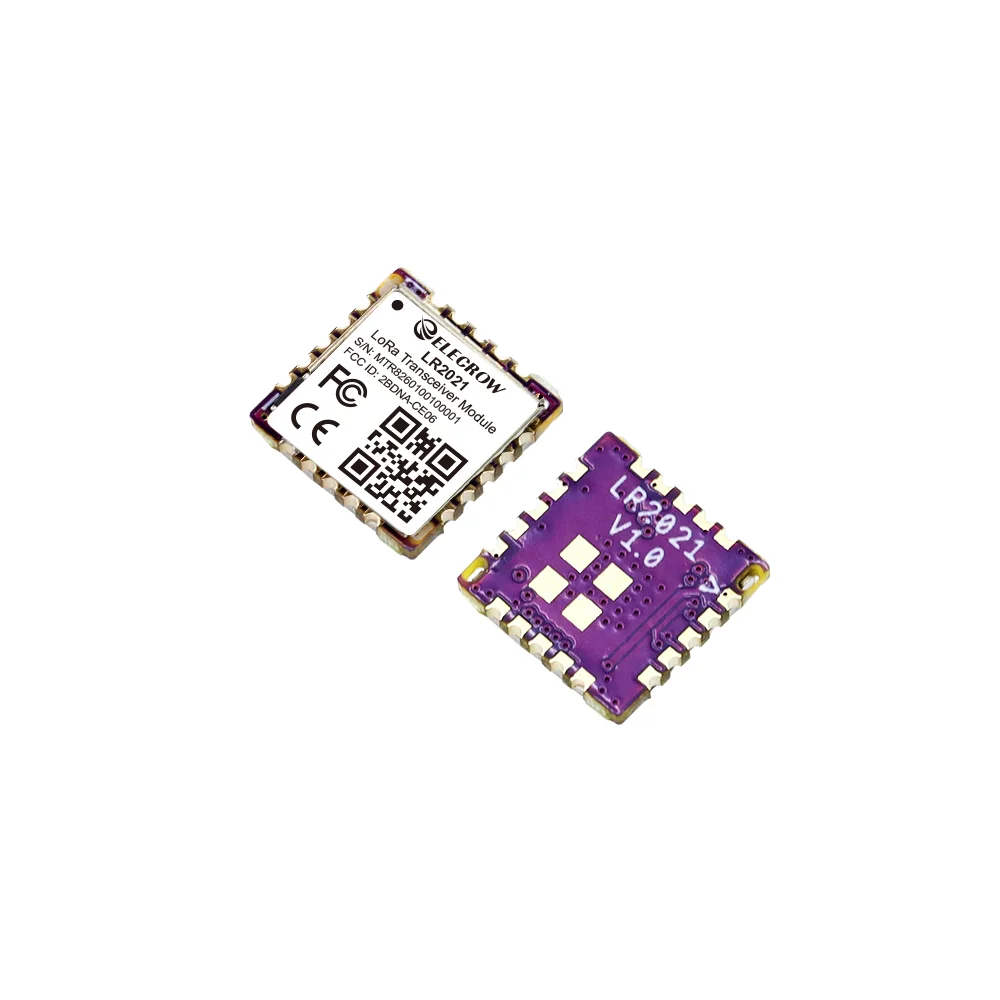
The LR2021 is a high-performance multiband wireless transceiver module based on Semtech's fourth-generation LoRa® IP. The module integrates the LR2021 RF transceiver chip, a 32 MHz industrial-grade TCXO, SIMO/LDO power management, an SPI control interface, and separate low- and high-frequency antenna ports. It supports Sub-GHz, 2.4 GHz ISM, and licensed S-Band frequencies, making it suitable for terrestrial networks and satellite IoT communications.
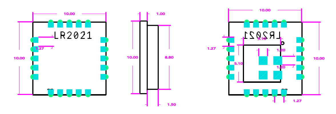
The module uses a 10 mm × 10 mm × 2.5 mm 20-pin SMT castellated package and is suitable for applications requiring a compact form factor, low power consumption, and multiregional deployment, including smart metering, asset tracking, industrial IoT, smart homes, smart cities, and satellite IoT.
Features
- Multiband connectivity: Sub-GHz coverage from 150–960 MHz, 2.4 GHz ISM coverage from 2400–2483 MHz, and support for S-Band satellite communication frequencies.
- High link budget: Sub-GHz receive sensitivity as low as -141.5 dBm (LoRa SF12, 125 kHz), maximum transmit power of +22 dBm, and a typical link budget of up to 163.5 dB.
- High-speed wireless transmission: FLRC data rates of up to 2.6 Mbps for OTA updates, image transmission, and reporting edge-computing results.
- Low power consumption: Typical chip-level sleep current of 0.47 µA without data retention and typical Sub-GHz receive current of 5.7 mA in non-boosted gain mode.
- Dual antenna ports: ANT_LF for 150–960 MHz; ANT_HF for 2.4 GHz ISM and S-Band. Both ports are designed for 50 Ω systems.
- Multiple modulation schemes: Supports modulation schemes including LoRa, (G)FSK, OOK, O-QPSK, LR-FHSS, FLRC, DBPSK, and BLE 5.0 PHY.
- Multiprotocol compatibility: Supports protocol ecosystems including LoRa/LoRaWAN®, Amazon Sidewalk, Sigfox, Wi-SUN, Wireless M-Bus, Z-Wave, BLE 5.0 PHY, and IEEE 802.15.4 (Thread/Zigbee).
- Long-range communication: The specifications indicate a typical Sub-GHz line-of-sight communication range exceeding 15 km and up to 68 km in open environments when using a high-gain antenna. Actual range depends on the frequency band, data rate, antenna, terrain, interference, and regulatory restrictions.
- Industrial operating temperature: -40°C to +85°C.
- Compact package: 10 mm × 10 mm × 2.5 mm, 20-pin SMT castellated package with a 1.27 mm pin pitch.
:::note Specific protocol features, frequency-band compliance, and available transmit power depend on the host software, antenna design, and regulatory requirements of the deployment region. :::
Applications
- Smart electricity, water, gas, and heat meters
- Global logistics, land and sea transportation, and valuable asset tracking
- Predictive maintenance of industrial equipment, factory environmental monitoring, and Mesh networks
- Smart home gateways, border routers, and end nodes
- Smart city applications such as streetlights, waste bins, geomagnetic parking detection, and environmental sensing
- LEO satellite IoT terminals for marine, desert, and emergency scenarios
- Mesh intercoms, drone data transmission, and wearable device synchronization
System Overview
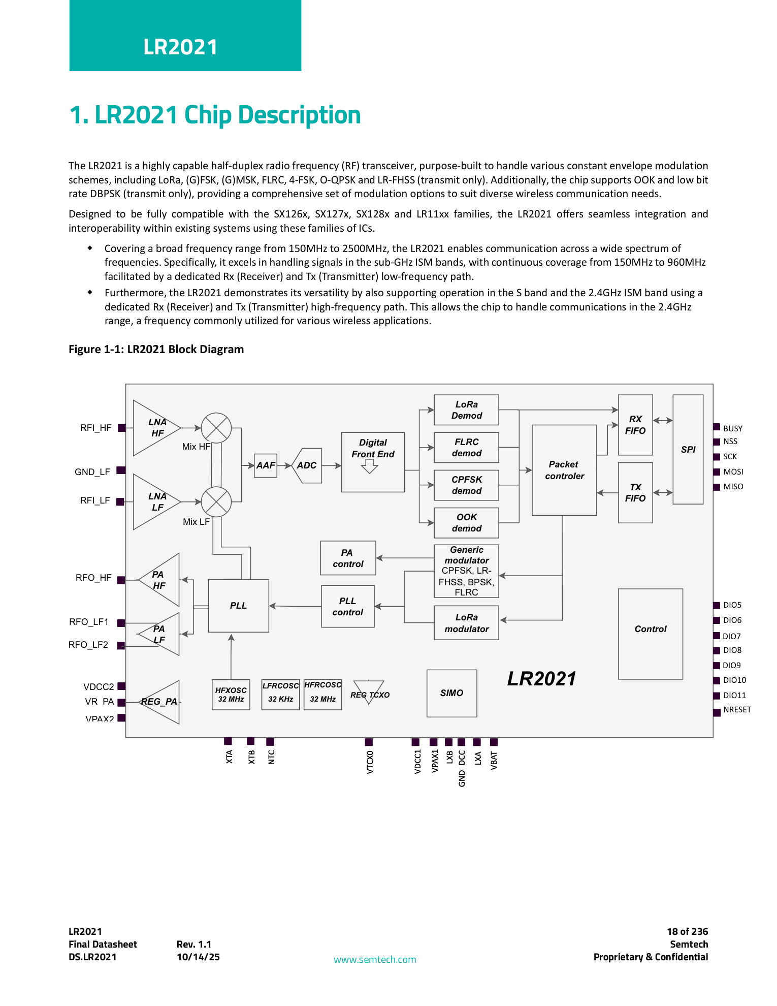
The LR2021 module is built around the Semtech LR2021 RF transceiver and integrates an RF front-end matching network, a 32 MHz TCXO, and power decoupling and management circuitry. The host MCU controls the module through the SPI interface and uses signals such as BUSY, NRESET, DIO5, DIO6, and TX/RX_EN for status monitoring, interrupts, reset, and RF front-end control.
The module has independent low- and high-frequency transceiver channels: ANT_LF corresponds to the Sub-GHz channel, while ANT_HF corresponds to the 2.4 GHz ISM and S-Band channels.
Specification
The following parameters were tested at VDD = 3.3 V, an ambient temperature of 25°C, and with a 32 MHz TCXO reference clock.
| Parameter Category | Parameter | Specification |
|---|---|---|
| Chip and Hardware | Main chip | Semtech LR2021 fourth-generation LoRa transceiver |
| Chip and Hardware | Operating voltage | 1.8–3.7 V, 3.3 V typical |
| Chip and Hardware | Operating temperature | -40 to +85°C |
| Chip and Hardware | Package dimensions | 10 mm × 10 mm × 2.5 mm, 20-pin SMT castellated package |
| Chip and Hardware | Reference clock | 32 MHz industrial-grade TCXO |
| Chip and Hardware | Antenna ports | ANT_LF + ANT_HF, 50 Ω |
| RF Transmit | Maximum Sub-GHz transmit power | +22 dBm |
| RF Transmit | Maximum 2.4 GHz transmit power | +12 dBm |
| RF Transmit | Transmit power dynamic range | 32 dB, in 0.5 dB steps |
| RF Receive | Sub-GHz receive sensitivity | -141.5 dBm @ LoRa SF12 / BW 125 kHz |
| RF Receive | 2.4 GHz receive sensitivity | -103 dBm @ O-QPSK 250 kbps DSSS |
| RF Receive | Typical link budget | 163.5 dB |
| Modulation | Supported modulation schemes | LoRa, (G)FSK, OOK, O-QPSK, LR-FHSS, FLRC, DBPSK, BLE 5.0 PHY |
| Modulation | LoRa spreading factors | SF5–SF12 |
| Data Rate | LoRa | 0.0458–125 kbps |
| Data Rate | FLRC | Up to 2.6 Mbps |
| Operating Band | Sub-GHz | 150–960 MHz |
| Operating Band | 2.4 GHz ISM | 2400–2483 MHz |
| Operating Band | Licensed S-Band | 1900–2200 MHz (satellite communications) |
| Digital Interface | Control interface | SPI, up to 16 MHz; digital I/O |
| Data Buffer | FIFO | Separate transmit/receive FIFOs |
Hardware Overview
Pinout
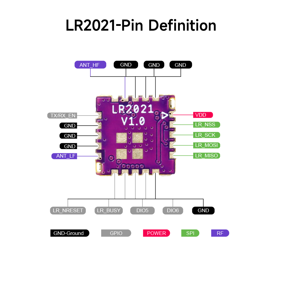
The LR2021 uses a 20-pin SMT castellated package. The top-view pin locations and signal groupings are shown below.
Pin Definitions
| Pin | Name | Type | Description |
|---|---|---|---|
| P1 | VDD | Power | 3.3 V power input; parallel 47 µF, 10 µF, and 100 nF decoupling capacitors are recommended |
| P2 | LR_NSS | Input | SPI chip select, active low |
| P3 | LR_SCK | Input | SPI clock |
| P4 | LR_MOSI | Input | SPI data input, host to module |
| P5 | LR_MISO | Output | SPI data output, module to host |
| P6 | GND | Power | System ground |
| P7 | DIO6 | Input/Output | Configurable as IRQ, RF_SWITCH, GPIO, HF_CLK_OUT, or TX/RX_TRIGGER |
| P8 | DIO5 | Input/Output | Configurable as IRQ, RF_SWITCH, GPIO, HF_CLK_OUT, or TX/RX_TRIGGER; pulled up by default after reset |
| P9 | LR_BUSY | Output | Busy status indicator; high indicates that the module is processing a command |
| P10 | LR_NRESET | Input | Active-low reset; hold low for at least 100 µs |
| P11 | ANT_LF | RF Input/Output | 150–960 MHz low-frequency antenna port, 50 Ω |
| P12 | GND | Power | System ground |
| P13 | GND | Power | System ground |
| P14 | GND | Power | System ground |
| P15 | TX/RX_EN | Input/Output | External RF switch or FEM control; may also be used as a general-purpose control signal |
| P16 | NC | - | No connection |
| P17 | ANT_HF | RF Input/Output | 2.4 GHz ISM and S-Band high-frequency antenna port, 50 Ω |
| P18 | GND | Power | System ground |
| P19 | GND | Power | System ground |
| P20 | GND | Power | System ground |
| P21–P24 | GND | Power | Ground pads on the bottom of the module; connect to the main ground plane using multiple ground vias |
Electrical Characteristics
Absolute Maximum Ratings
:::warning Exceeding the absolute maximum ratings may cause permanent damage to the device. Prolonged operation near these limits may reduce device reliability and service life. :::
| Symbol | Parameter | Minimum | Typical | Maximum | Unit |
|---|---|---|---|---|---|
| VDDmr | Supply voltage | -0.5 | - | 3.9 | V |
| Tmr | Temperature | -55 | - | 125 | °C |
| Pmr | Maximum RF port input power | - | - | +10 | dBm |
Recommended Operating Conditions
| Symbol | Parameter | Minimum | Typical | Maximum | Unit |
|---|---|---|---|---|---|
| VCC | Supply voltage | 1.8 | 3.3 | 3.7 | V |
| Top | Operating temperature | -40 | - | +85 | °C |
| Tmaxj | Maximum junction temperature | - | - | 105 | °C |
| Clop | Digital port load capacitance | - | - | 20 | pF |
| VSWR | Standing-wave ratio for guaranteed PA stability | - | - | 10:1 | - |
Power Consumption
| Mode | Condition | Typical | Unit |
|---|---|---|---|
| Sleep | No data retention, no RTC | 0.47 | µA |
| Sleep | Data retention, no RTC | 0.57 | µA |
| Sleep | Data retention, RTC enabled | 1.4 | µA |
| Standby RC | Internal 32 MHz RC oscillator enabled | 1.21 | mA |
| Standby XOSC | 32 MHz crystal/TCXO enabled | 1.79 | mA |
| Frequency Synthesis | 915 MHz | 3 | mA |
| Receive Sub-GHz | Non-boosted gain | 5.7 | mA |
| Transmit Sub-GHz | +22 dBm | 105 | mA |
| Transmit Sub-GHz | +17 dBm | 43 | mA |
| Transmit Sub-GHz | +14 dBm | 27 | mA |
| Transmit Sub-GHz | +10 dBm | 17 | mA |
| Transmit 2.4 GHz | +12 dBm | 23 | mA |
Mechanical Characteristics
The module measures 10 mm × 10 mm with a typical thickness of 2.5 mm; the peripheral castellated pins have a pitch of 1.27 mm. The recommended pads should match the module pins, and a ground pad should be provided beneath the module to improve RF grounding and heat dissipation.
Recommended PCB Layout
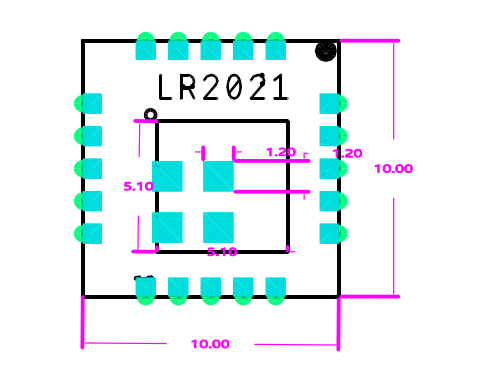
- ANT_LF and ANT_HF traces should be as short as possible and maintain a 50 Ω characteristic impedance.
- Do not place copper pours or signal traces beneath the antenna and RF trace areas; reserve an RF keepout area.
- Power-supply decoupling capacitors should be placed close to VDD, with leads and return paths kept as short as possible.
- The RF matching network should follow the Semtech reference design, with L/C components placed close to the corresponding RF ports.
- The ground pad beneath the module should be connected to the main ground plane using multiple vias to reduce ground impedance and improve heat dissipation.
- SPI, reset, and status signals between the host and the module should not run parallel to RF traces over long distances.
Getting Started
1. Hardware Requirements
- 1 LR2021 module
- 1 host MCU supporting 3.3 V logic levels
- A regulated 3.3 V power supply with sufficient headroom for peak transmit current
- A 50 Ω antenna and matching network for the target frequency band
- An SPI interface and at least 4 control/status GPIOs
- An oscilloscope, logic analyzer, or current analyzer for prototype debugging (optional)
2. Connect the Host MCU
At a minimum, the host must connect the following signals:
| LR2021 Signal | Host Connection | Description |
|---|---|---|
| VDD | 3.3 V | 47 µF + 10 µF + 100 nF decoupling capacitors placed near the module are recommended |
| GND | GND | Reliably ground all GND pins and bottom ground pads |
| LR_NSS | SPI CS | Active low |
| LR_SCK | SPI SCK | SPI clock up to 16 MHz |
| LR_MOSI | SPI MOSI | Host transmits, module receives |
| LR_MISO | SPI MISO | Module transmits, host receives |
| LR_BUSY | GPIO input | Do not send new commands while high |
| LR_NRESET | GPIO output | Active-low reset; hold low for at least 100 µs |
| DIO5 / DIO6 | GPIO input/output | Configure as interrupt, RF switch, or trigger signals according to the firmware |
| TX/RX_EN | GPIO or external FEM | May be configured for the application when no external RF switch is used |
3. Connect the Antennas
- For Sub-GHz operation, connect a 150–960 MHz 50 Ω antenna or matching network to ANT_LF.
- For 2.4 GHz or S-Band operation, connect a 50 Ω antenna or matching network for the corresponding frequency band to ANT_HF.
- When routing both frequency bands on the same PCB, ensure that the two RF traces are isolated from each other to prevent coupling.
- Do not transmit at high power without an appropriate load or antenna connected.
4. Power-on Checklist
- Before applying power, confirm that VDD does not exceed 3.7 V and check for shorts between the power supply and ground.
- Confirm that ANT_LF and ANT_HF are not interchanged and that the connected antennas cover the target frequency bands.
- Pull LR_NRESET low for at least 100 µs, then release it.
- Wait for LR_BUSY to be released before sending initialization commands over SPI.
- First verify SPI, reset, interrupt, and frequency configurations at low transmit power, then gradually increase the power.
- Use a spectrum analyzer or calibrated receiver to confirm that the center frequency, output power, and modulation parameters comply with local regulations.
:::note Module register commands, driver APIs, and LoRaWAN protocol stack integration should follow the Semtech LR2021 datasheet and corresponding software package. :::
Reference Design
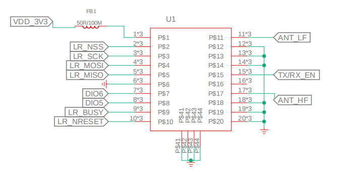
A typical application includes a 3.3 V power input, an SPI control interface, DIOs, dual antenna connections, and RF port protection. The following reference design is provided with the module documentation.
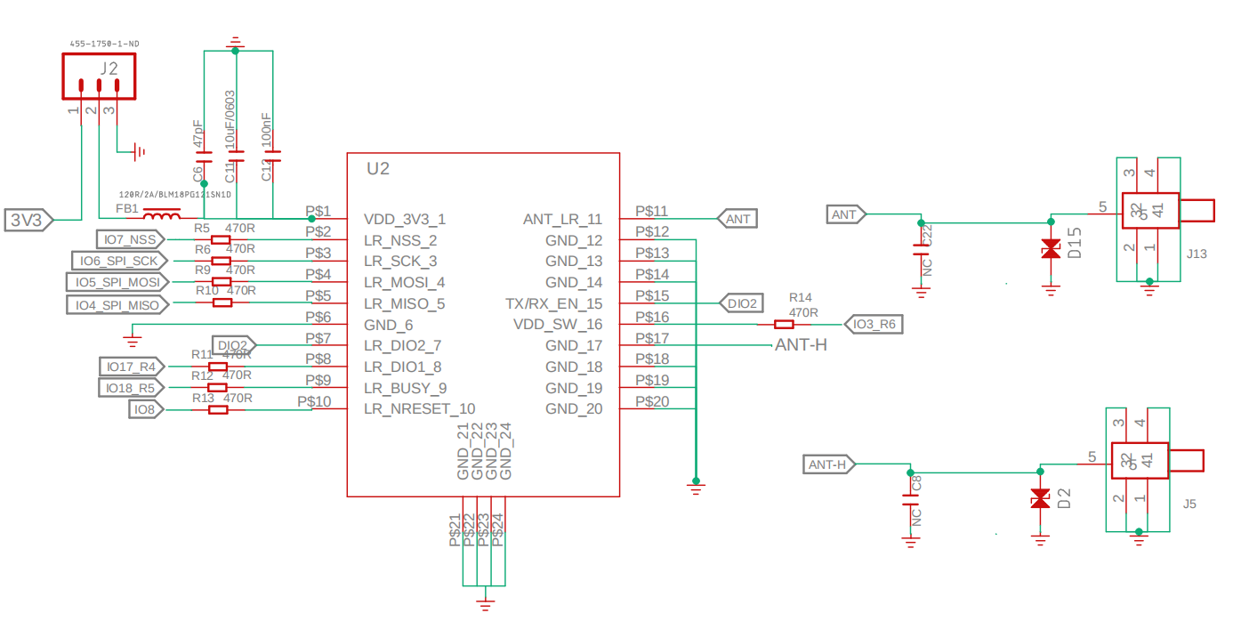
Observe the following design considerations:
- 47 µF, 10 µF, and 100 nF multistage decoupling is recommended at the VDD input.
- The reference design uses 470 Ω series resistors on the SPI and certain control lines to suppress reflections and EMI; actual resistance values should be determined based on the host drive capability, trace length, and signal-integrity testing.
- LR_NRESET should be pulled up to VDD through a 100 kΩ resistor.
- ANT_LF and ANT_HF should each use a 50 Ω matching network designed for the target frequency band.
- Low-parasitic TVS/ESD devices may be added to the RF ports; their impact on insertion loss and impedance matching must be evaluated during component selection.
Resources
Product
Hardware Files
Related Documents
- Semtech LR2021 Datasheet Rev. 1.1
- LoRaWAN® Regional Parameters v1.0.3
- AN1200.102 LR2021 TCXO Temperature Compensation Application Note
Revision History
| Date | Version | Description |
|---|---|---|
| 2026-10-08 | V1.0 | Initial Wiki version compiled from the LR2021 module specifications, schematic, and PCB documentation |
Tech Support and Product Discussion
If you encounter any issues while using the service, you can contact us via the social media links in the bottom-right corner of elecrow or send an email to techsupport@elecrow.com for technical support.